An Overview of \(S\) parameters in RF and Microwave Engineering
RF and microwave equipment is typically designed using self contained sub-units, generically called 'networks', connected together to build the hardware for a particular function. Every network must have one or more ports and must, according to the original \(S\) parameter definition, behave linearly [6] [7] [11]. A simple network may have just one port, such as an oscillator or an antenna if it is a source, or it may be some form of load such as a detector or an analog to digital converter (ADC). Most networks have 2 or more ports. Typical hardware usually comprises several networks like these connected together. Furthermore, the transmission lines necessary to connect the networks are each considered to be 2 port networks. These could be any of many different types: single ended or differential, for example coaxial cables, microstrip, coplanar strips or stripline, in fact whatever is appropriate for the frequencies and physical hardware in use. An example schematic of a piece of RF or microwave equipment comprising interconnected networks is shown in Figure 1-1.
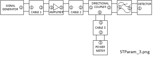
This example demonstrates how networks may typically be connected together port to port. The ports of each network have been numbered serially by the circled numbers starting with 1, usually at the input. Initially, we will consider the ports to be unbalanced or single-ended of nominal impedance 50 \(\Omega\). We will consider balanced ports and different impedances later. There is no specific requirement for \(S\) parameter port numbering but they must be uniquely identified. Port numbering like this ensures that the network ports are connected together unambiguously when the equipment is assembled and enables reliable simulations with traceability. The port numbers should be allocated for each network stand-alone before any measurements are performed. Typically, a correctly set up and calibrated vector network analyzer (VNA) would be used to measure the \(S\) parameters [15] [16].
A port is defined as a 'two wire' interface to the network which may connect to any external components such as other networks, signal sources, loads, amplifiers or test equipment [2] [11] [12]. Historically, these are often called 'terminals' despite the fact that the traditional concept of physical terminals may not be appropriate at higher frequencies. At each of the port interfaces in Figure 1-1 two 'wire' connections are therefore shown. For simpler schematics, the network port connections may be reduced to single lines, provided they are properly described.
The terminal pairs might look like differential connections (differential pairs), but that is not necessarily the case. Despite the trend towards differential transmission lines in recent years, in fact the majority of connections like these are unbalanced, typically coaxial cable or microstrip. Coaxial connections are single-ended in which the screen or shield connections are all assumed to be 'at the same potential' and connected to ground. As operational frequencies have increased over the years, this assumption has become less accurate and sometimes results in electromagnetic compatibility (EMC) problems, unwanted radiated emissions and susceptibility.
We have to be cautious when allocating and using port numbers however, because those used will relate directly to the element subscripts within the associated \(S\) parameter matrix. For example, 'CABLE 1', a 2 port transmission line, in Figure 1-1 is nominally a passive reciprocal network [3]. It was designed to be useable with the signals passing in either direction. The equipment will probably appear to work satisfactorily if it was connected in reverse to that shown, with port 2 on the left and port 1 on the right. However, any precision cascade analysis required would then require modification of its \(S\) parameter matrix, to interchange the \(S\) parameter indices 1 to 2 and vice versa. Unfortunately, no manufacturer will ever produce a perfectly reciprocal cable and elements of non-reciprocity may become significant, especially at higher frequencies.
Transmission Lines and Imperfect Matching
\(S\) parameter theory calls heavily on the equations associated with transmission lines, or more precisely, transmission lines which are imperfectly matched [2] [13]. In fact, the adjective 'scattering' used in 'scattering parameters' comes from the scattering of propagating plane waves when they pass across media which have differing impedances and are therefore unmatched. This may be a better analogy in the optical domain where phenomina such as diffraction are well known and more easily observed.
We often require a source to be 'perfectly matched' to a load for maximum power transfer across our frequency range of interest. That is of course impossible to achieve, but we can usually get much closer to it with the correct application of \(S\) and \(T\) parameters. A more verbose description might be 'the best reasonable match across an adequate frequency range'.
\(S\) Parameter Matrices
The electrical performance of every network, such as each of those shown in Figure 1-1, may be expressed as an \(S\) parameter matrix of dimensions \(N \times N\), where \(N\) is the number of ports of the network [1] [7] [14]. As an example, let us take the amplifier. (OK, refer to it as a network if you prefer). Considered in isolation we will call this the device under test (DUT). Its ports are numbered 1 and 2 for the input and output respectively. The DUT would have been designed and then tested using a correctly set up and calibrated VNA, for full 2 port measurements across the required frequency range, let us assume 1.0 \(GHz\) to 1.5 \(GHz\) in 10 \(MHz\) steps[2] [15] [17]. That is a total of 51 steps including the start and end frequencies. \(S\) parameters are always functions of frequency and very often of other parameters as well such as temperature, DC voltage and bias, control voltage and so on, so these must all be recorded along with the measurements.
After the measurement, the VNA will yield a set of data, 2 port \(S\) parameter measurements, for a set of discrete CW frequencies, in this case 51. At this point the \(S\) parameter indices for the DUT allocated by the VNA, usually 1 and 2 for a 2 port VNA, must be correctly related to the DUT. So, for example, if the VNA ports 1 and 2 were connected to the amplifier (or DUT) ports 1 and 2 respectively, the default \(S\) parameter indices of the VNA would be correct. If the DUT had different port numbering, the VNA output data would require correction, changing the '1' and '2' indices to whatever was required.
For every frequency step, the VNA will internally generate a \(2 \times 2\) \(S\) parameter matrix which will comprise an array of 4 values representing the measured (linear) magnitude and the (spatial) phase of the parameter concerned. Each element of the matrix will be represented in the form \(S_{mn}\), where \(m\) is the row and \(n\) is the column of the associated \(S\) parameter matrix. The subscript indices, \(m\) and \(n\), represent the 'response' port and the 'stimulus' port indices respectively. For example, \(S_{mn}\) represents the \(S\) parameter result for a stimulus applied at port \(n\) and the response measured at port \(m\) whilst the other port(s) terminated in precisely the system impedance.
An example of an \(S\) parameter matrix result at one frequency for a 2 port network in a few different formats is shown by the 2×2 matrix in (1-1).
Any of the \(S\) parameter matrix forms is perfectly valid. Notice that the complex exponential form does not include the 'real part' operator 'Re'. This is common practice in electrical engineering to represent complex exponential waveforms.
The \(S\) parameter values, elements in the \(S\) parameter matrices, have been defined to relate directly to common RF parameters: reflection coefficient (from which are derived return loss and VSWR) and transmission from one port to another port (gain and reverse isolation). In fact, reflection coefficient may be considered as transmission from one port (an incident or forward wave) to the same port (a reflected wave). Referring again to the \(S\) parameter index notation, \( S_{mn} \): for \( m = n \) the result is a reflection coefficient at port \(m\) or \(n\). For \( m \ne n\) the result represents transmission from port \(n\) to port \(m\).
\(S\) parameter measurements also require a defined nominal system impedance. This is most conveniently the same as the nominal system impedance of the equipment under test, commonly 50 \(\Omega\) exactly, non-reactive. However, it is possible to convert \(S\) parameter measurements from one system impedance to another. A common example would be between 50 \(\Omega\) and 75 \(\Omega\), unbalanced coaxial in both cases, as both impedances are used in some communications systems.
\(S\) Parameter Definitions
In (1-1) and all other \(S\) parameter matrices, the columns represent the stimuli ports and the rows represent the response ports. So, for example, \(S_{21}\) represents the result for a stimulus applied to port 1 and the response measured at port 2. \(S_{22}\) would represent both the stimulus being applied to port 2 and the response being measured from port 2.
In every measurement by definition, every port must be terminated exactly in the system impedance \(Z_{0}\), a purely resistive value. This must not change across the whole measurement frequency range. These conditions also apply to VNA source and load impedances during the normal measurement procedure, and to the loads connected to any unused ports. If the equipment under test has more ports than those available on the VNA, the tests must be performed in stages. For example, if the VNA has 2 ports, only 2 ports may be measured at a time, on each occasion every unused DUT port must be terminated in the exact system impedance.
Caution may be required with port numbering. By convention, these normally correspond to the indices (row and column numbering) of the \(S\) parameter matrix so, in (1-1), the port numbers allocated were 1 and 2. However, there may have been some very logical reason why the ports might have been numbered 34 and 92 instead, in which case the corresponding \(S\) parameter matrix would be (1-2). This would be fine provided it was still only a 2 port network. If it was actually a 3 port network with ports 34, 92 and 97 for example, then the true \(S\) parameter matrix would need to have 3 dimensions \(3 \times 3\) with the rows and columns named 34, 92 and 97.
\(S\) Parameter Definitions for a 2 Port Network
We will consider the \(S\) parameters of a 2 port network which may have either balanced ports, or unbalanced ports. Both examples are shown schematically with voltages and currents in Figure 1-2. A netwowrk with coaxial connectors will have, by definition, unbalanced ports.

2-port networks are the type most commonly encountered. Most VNAs also have 2 ports. Therefore, once set up and calibrated, these enable a whole set of 2 port \(S\) parameter measurements in one operation. Either port of a two port VNA may also be used to measure the \(S\) parameters of a one port networks such as a load. The performance of a one port source, such as a signal generator, cannot be described by \(S\) parameters because it contains a source and therefore cannot meet the \(S\) parameter measurement criteria. The \(S\) parameters of a network with 3 or more ports can be measured by a 2 port VNA in stages, 2 ports at a time.
In general, at each port there will not be a perfect match so there will be a forward wave component into the port and a reverse wave component out of the port. These are represented respectively as \(V_{n F}\) and \(V_{n R}\) where '\(n\)' is the port identity shown in Figure 1-2 by a number enclosed in a circle. So for example the forward wave at port 2 will be \(V_{2 F}\) and the reverse wave at port 1 will be \(V_{1 R}\). For this imperfect match condition at port '\(n\)' a standing wave will occur with the total (resultant) voltage \(V_n\) and resultant current \(I_n\) given, using transmission line theory, by the equations in (1-3).
\(Z_0\) is the system impedance in ohms (\(\Omega\)). For each port we may define incident and reflected waves which are sometimes called 'power waves', \(a_n\) and \(b_n\) respectively, where 'n' is the port identity. Each of these is a complex value according to the definition in (1-4).
To re-iterate, \(Z_0\) is the defined system impedance, a purely resistive value such as 50 Ω, or to be more explicit, as we are using complex parameters, \(Z_0 = 50 + j0 \) Ω.
A common question is: "How does the VNA present 'exact' \(Z_0 = 50 + j0 \) Ω impedances to the DUT during measurements, especially across big frequency ranges?" [15] [16] [17] [18]. Of course it cannot, but today's even quite basic VNAs include very powerful and fast processing capability which is heavily exploited. During the calibration procedure this is used to calculate and correct for systematic errors inherent in the VNA itself and the necessary cables and/or adaptors [17] [18] [19]. The resulting 'corrected' measurements then significantly account for departures of the source and load impedances from the nominal values.
Let us consider a 2 port network as an example on which the ports are identified as 1 and 2. As with all network parameters, there are no rules about which port may be an input or an output but whatever is chosen should be related to the DUT in some way, such as with labels, but ideally with proper traceable handware identification. When such measurements are planned, an initial assessment must be made to accommodate any high power levels which may exit any port to avoid possible test equipment over-stressing or damage. This should include the possible consequences of fault conditions which may occur such as instability (oscillation).
For example, if we were planning to measure the \(S\) parameters of a 10 \(W\) linear amplifier, it would be risky to connect its output port directly to a VNA whose maximum incident power was, say, +30 \(dBm\) (1 \(W\)). Even if we had taken special precautions to reduce the input power to give an expected output power well below +30 \(dBm\), a 10 \(W\) output power might have been caused by unforseen instability. This would likely cause expensive damage to the VNA and put it out of service for repair.
Further to (1-3) and (1-4), the relationship between the power waves, \(a_n\) and \(b_n\) for the 2 port \(S\) parameter matrix is given by (1-5).
Expanding the matrix equation in (1-5) gives the two equations in (1-6). These show the relationships between the 2 port \(S\) parameter matrix and the incident and reflected power waves, \(a_n\) and \(b_n\), for each of the ports.
All of the definition equations so far have assumed that every port is terminated exactly in the system impedance, \(Z_0\), either a source or load as required. Consider port 2 of the 2 port network. If this was connected to a load of exactly \(Z_0\), there would be no reflections from the load by our definition and therefore no incident wave at port 2, so \(a_2\) would be zero. Substituting this into the equations in (1-6) yields the results \(S_{11} = b_1 / a_1\) and \(S_{21} = b_2 / a_1\). By similar arguments for loading port 1 with \(Z_0\), expressions are obtained for all of the 2 port \(S\) parameters which are shown in (1-7).
The function of the VNA is to accurately measure the power waves, in magnitude and phase, at each of the ports separately at every frequency. Then the VNA must perform the necessary calculations from (1-7) to obtain the associated S parameters. This is achieved after correctly setting up and calibrating the instrument.
What is a Network?
A network in the context of \(S\) parameters is a number of interconnected electrical components designed to provide a function and to operate across a range of frequencies. The connections do not necessarily require to be Galvanic, for example it may include capacitors and/or transformers. A network may be passive or active but to comply with the \(S\) parameter conditions it must behave linearly and this normally means under small signal, steady state conditions. An active network is defined as one in which external non-signal power is required in order for it to operate. In this context, 'small signal' means low power continuous wave (CW), at one or more frequencies. \(S\) parameters can also be specified under non-linear conditions. This is not recommended but, provided the conditions under which they are measured are accurately known and repeatable, they may provide useful information. A network may have one or more ports. Networks with one, two or three ports are the most common.
What is a Port?
A port is defined as a pair of terminals connected to defined nodes on the network through which the signal currents may flow in either direction. The algebraic definitions of the forward and the return power flow directions are as identified in Figure 1-2. Each pair of terminals comprises two conductor connections designed appropriately for the frequencies being used. Typically, for single ended ports, these might be coaxial connectors or microstrip connections.
How Many Ports May a Network Have?
Any number. The largest I have seen is 65 for a component used in a phased antenna array application. Fortunately the ports were serially numbered 1 to 65.
That 65 Port Thing Was Surely Not One Network But Several Small Ones Wasn't It?
No, it was literally one network according to the circuit schematic. There was a physical RF connection path (ie. not necessarily Galvanic) from any port to any other port. There may have been unintentional leakage paths between some of ports which would have been included in the results but that does not change anything. The purpose of S-parameter measurements is to characterise networks including imperfections to determine if they are acceptable. If not, further design/development work can be performed to correct them. With some of the latest test equipment and very careful VNA setup and calibrations it is possible to measure isolation values to greater than 100 \(dB\). That would correspond to a log magnitude \(S\) parameter transmission measurement of less than -100 \(dB\), since (linear) transmission is the reciprocal of (linear) isolation. So the VNA is capable of measuring, for example, extremely small values of leakage which might have been caused by capacitive coupling between tracks, ground planes and other conductors.
What Are Balanced and Unbalanced Networks?
Alternatively, these could be referred to as 'differential' or 'single-ended' networks respectively. Schematics of both types are shown in Figure 1-2 [20]. More precisely we should refer to balanced or unbalanced ports rather than networks. That is because, within a network the circuit topology may include portions with a variety of topologies most appropriate to the circuit design: balanced, unbalanced or quasi-balanced. For the network nodes from which external connections are made to the ports, the circuit normally has to be adjusted to some form of standard electrical architecture appropriate for connecting to external equipment, for example standardised connectors.
Every port interface requires two conductor connections, or terminals, to allow power to flow into or out of the network as appropriate. There is no assumption of any Galvanic (DC path) common connection between two or more port terminals of the network, such as that often provided by a 'ground'. However, most VNAs and other test equipment do have single ended (unbalanced, coaxial) ports of which one terminal, the screen or shield, is grounded by definition. It is not possible to use one of these directly to make any balanced measurements of a network. There are some options available for mixed mode (balanced and unbalanced) \(S\) parameter measurements using a 4 port single ended VNA with a special calibration [5]. These will be described in Section 2.6. In these cases the system impedances of the common mode and differential mode measurements are 25 \(\Omega\) and 100 \(\Omega\) respectively.
How Do You Interpret 'Linear' and 'Logarithmic Magnitude' \(S\) Parameter Measurements?
So far we have mathematically only considered linear \(S\) parameters. All \(S\) parameters are expressed as unitless complex values because they are derived from the ratios of two complex numbers with the same units, the power waves, such as those shown in (1-7) for a 2 port network [7]. We can see from (1-4) that the rather unusual units for power waves are volts per square root of impedance (\(V / \sqrt{\Omega} \)). Every \(S\) parameter therefore has an amplitude and a (spatial) phase and may be represented in rectangular, polar or exponential form. An example of each of these is shown in (1-1). Linear amplitude (or magnitude) may be obtained directly from the value \(R\) in either the polar or the exponential forms. It may be obtained from the rectangular form by squaring the real and imaginary coefficients, adding them and then taking the square root of the result. (1-8) shows each of the resulting generic \(S\) parameter for \(S_{mn} \), the linear magnitude (\(R\)) and phase (\(\phi\)) forms.
The (complex) exponential format shown in (1-8) may be converted to the rectangular form by using Euler's equation (1-9).
Log magnitude is an abbreviation of logarithmic magnitude, say \( R_{LM} \) normally using the decibel (dB) scale definition. (1-10) shows how the log magnitude value may be derived from the magnitude of an \(S\) parameter of the form \(S_{mm}\). The log coefficient in this case is 20 because all \(S\) parameters are derived from voltages and currents, as shown in (1-3), (1-4) and (1-7). Use of the \(dB\) and derived scales is widespread in science and engineering because it simplifies handling parameter values covering many orders of magnitude.
In Section 1.2 we defined \(m\) and \(n\) to be the row and column indices of the \(S\) parameter matrix respectively, so the condition \(m = n \) is allowed. We will see in Section 1.11.3 that \(S\) parameters of the form \(S_{mm}\) or \(S_{nn}\) are equivalent to the voltage reflection coefficient \( \rho\ \) from the same port, \(m\) or \(n\) as appropriate. Although there is a 'current' reflection coefficient, the voltage version is more common and usually simply referred to as reflection coefficient. Since the network is defined to be linear, it must be stable and not oscillating. Therefore, the magnitude of the reflection coefficient \(|\rho|\) must in general be less than one. It will equal one in the case of a perfect open circuit or short circuit.
Other Parameters Related to \(S\) Parameters
A correctly set up and calibrated vector network analyzer (VNA), once connected to the DUT, will return large volumes of precision \(S\) parameter and other characterisation data. This may be readily converted into many of the parameters frequently used in RF and microwave engineering. Some are included below followed by fuller descriptions.
- Transmission or Gain
- Phase
- Reflection Coefficient
- Return Loss
- Voltage Standing Wave Ratio (VSWR)
- Rollett Stability Factor
Transmission or Gain
The transmission of a network from one defined port to another is another name for its gain [7]. If phase is not required it implies the transmission magnitude of a network which has at least 2 ports which are identified and correctly related to the \(S\) parameter indices. We will assume that port 1 is the input (connected to the stimulus or source) port and port 2 is the output (connected to the response device or load). The stimulus and response devices would normally be internal to the VNA. It is understood to mean either the linear (unitless) transmission (\(G\)) or the logarithmic (\(dB\)) transmission (lower case \(g\)). The equations for both types are shown in (1-11).
Transmission Phase
In the context of \(S\) parameters, transmission spatial phase is normally referred to simply as 'phase', say \(\phi\). The temporal component of phase, say \(\theta\), where \(\theta = \omega t = 2 \pi f t \) is removed by the \(S\) parameter VNA calibration procedure at each of the test frequencies before the measurement. Two formulas relating to phase were presented in (1-8) and are repeated here in (1-12). Again we will assume that ports 1 and 2 are the input and output ports respectively, also \(c\) and \(d\) are the real and imaginary coefficients of \(S_{21}\) respectively.
The VNA may have features to display phase data in either 'wrapped' or 'unwrapped' and to calculate related parameters such as delay.
Reflection Coefficient
The reflection coefficient, actually the voltage reflection coefficient, which we will call \(\rho\) is measured at a single port and is defined as the ratio of the reflected voltage \(V_R\) to the forward voltage \(V_F\) (1-13). As both are complex quantities, \(\rho\) is also a complex quantity.
Assuming we require the result at port 1 (\(m = n = 1 \)), then \(S_{11}\) has the same definition as \(\rho\) (1-13). Here we will re-name it as \(\rho_{11}\) to associate it with \(S_{11}\). We can see this using the results from (1-4) and (1-7), summarised in (1-14).
If the network has more than one port, a similar argument applies for each of the other ports, for example \(\rho_{22}\), \(\rho_{33}\) etc.
Return Loss
Return loss is a scalar parameter measuring the reflection from a port so it does not include phase. By definition, it is a logarithmic measure, normally expressed in \(dB\), of the magnitude part of voltage reflection coefficient which was described in Section 1.11.3. We will use the symbols \(RL_{11}\), \(RL_{22}\) for the return loss at port 1 and port 2 respectively, and similarly for the other ports. (1-15).
Since it is defined as a loss as opposed to a gain, a negative sign is included. The coefficient of 20 is used because it is derived from voltage parameters. A return loss value of 0 \(d B\) represents a 100% reflection (a perfect short-circuit or open-circuit). As the match improves so the return loss value increases.
Voltage Standing Wave Ratio (VSWR)
Voltage standing wave ratio (VSWR) provides a similar scalar measure of the reflection from a port as Return Loss but VSWR is a linear measure of the standing wave so is unitless. The VSWR symbol is lower case '\(s\)', not to be confused with the upper case '\(S\)' used for \(S\) parameters. VSWR is defined as the sum of the magnitudes of the forward and reverse voltage magnitudes divided by their difference (1-16).
The VSWR for a perfect match is one, or 1:1 in ratio form, and for a perfect open or short circuit, it is infinity. The VSWR scaling is often more convenient to use than return loss for specifying well matched requirements, such as those required at a high power load or antenna.
Rollett Stability Factor
TBA
What is a Vector Network Analyzer?
A vector network analyzer (VNA) is an instrument designed to analyze the RF and microwave parameters of networks, in terms of transmission and reflection, across frequency. Precision VNAs are expensive instruments and represent a significant asset. The running costs are also high: yearly traceable calibration, calibration kits, precision cables, adapters, low VSWR loads, electronic calibration modules, cables, jigs, adapters and skilled operators. A VNA may not be economic to own unless it needs to be used regularly, otherwise rental of a suitable instrument might be an option.
Some common VNA features are listed below.
- Frequency Range, Number of Ports, Types and Genders
- Calibration for Correction of Systematic Errors
- Results Reporting and Data Output
- Swept CW and Pulse Capability
- Instrument Control and Data Acquisition
- Mixed Mode Capability
- External adjustments for High and Low Power Modes
- Options
Frequency Range, Number of Ports, Types and Genders
Most VNAs have precision coaxial connectors appropriate to the maximum operating frequency. In general, coaxial connectors have smaller diameters when specified for higher frequencies to avoid generation of non-transverse propagation modes. Connector genders must be selected to minimise the number of adapters, cables and their lengths required for the intended measurement. Unnecessary adapters, even low VSWR types, can degrade measurement uncertainties significantly. Most VNAs have 2 ports but these may be used to measure networks with any number of ports provided the correct procedures are followed. Whilst a VNA with just one port could exist, its function would be limited as it would only be capable of measuring one \(S\) parameter and may be described as an impedance meter.
Calibration for Correction of Systematic Errors
This is not the regular traceable equipment calibration and checks required for quality assurance, typically performed every 1 or 2 years. This is the internal VNA instrument calibration procedure usually done immediately before performing a measurement to correct for systematic (inherent and repeatable) errors present in the test equipment hardware [16] [17]. These include imperfect coupler directivity, source and load mismatch and frequency dependent variations. The data processing capability of most modern precision VNAs usually includes several calibration features. Once a calibration is completed, provided the equipment and environment are not disturbed, the calibration results may be saved and recalled later for similar measurements. Typically it is recommended that this type of calibration is repeated for a minimum frequency of once per day.
Results Reporting and Data Output
Modern VNAs usually provide many ways that results may be displayed on the instrument for immediate feedback to the operator, for example rectangular, polar, Smith chart and tabular forms with various scaling options. All results may be saved to internal and external memory types or exported for later processing. Most measurements will be 'corrected' meaning that a systematic error calibration has been performed and applied to the output as described in Section 2.2 [17]. 'Uncorrected' measurements may be adequate in some situations, for example setting up before formal measurements, if the reduced VNA accuracy can be tolerated. Data reporting or exporting is standard on most VNAs including industry standard file formats and high speed 'binary' modes. It is recommended to save all measurements in an electronic format such as one of these.
Swept CW and Pulse Capability
Components designed for operation with pulsed modulated waveforms, such as those used with radar equipment, usually have to meet different criteria from those designed for CW or near-CW waveforms. This results from handling different peak to mean power ratios (PMPR). The PMPR is effectively 1 for a continuous wave (CW, sine squared mean power) waveform but can be as high as 1000 for a pulsed CW primary radar, depending on the definition used. It would be very wasteful and expensive to design a radar DUT assuming the peak power in the same way that we assume mean CW power only on non-radar equipment. Due to thermal dissipation, it can be designed for the mean power which, in our example would be 1/1000 of the peak power and much easier to do. However, it must still be sufficiently resilient to handle the necessary voltage pulses without suffering any damage due to dielectric breakdown as this is a short-term phenomina.
VNA \(S\) parameter measurements have traditionally been performed by frequency swept CW, with linear or perhaps logarithmic frequency scaling for larger frequency ranges. The mean power level of the swept CW waveform is levelled accurately appropriate to keeping the DUT operating comfortably within its linear region. In many types of communications equipment this represents a reliable and representative test method. However, the power level incident at the DUT port must be carefully assessed. It must be appropriate for the DUT power supply, linear operation, heat sinking and avoiding any risk of dielectric breakdown. This should be representative of the mean power level the DUT would expect to handle in normal service. Swept CW is narrow band with perhaps a little frequency spread caused by the sweeping function and phase noise.
Some VNAs have swept pulse capability as well as swept CW. The main difference with swept pulse compared to swept CW is the larger spectrum occupied by the pulse waveform and its associated peak power. Otherwise, the same swept CW calibration procedure for systemic errors may be followed [18]. These must be processed correctly by the VNA with that capability. Correctly set up pulse tests are appropriate for DUTs which are designed to handle pulse waveforms. \(S\) parameters may be measured similarly to those using swept CW but the full pulse parameters must of course be recorded with the \(S\) parameter results.
Remote Instrument Control and Data Acquisition
Nearly all modern test equipment including VNAs are equipped with generations of Ethernet (IEEE 802.3) derived LAN capability with the 'Gigabit' version currently being the most popular standard. Because test equipment is such a significant investment, these hardware assets are often retained for many years and the data acquisition technology it incorporates sometimes becomes rather mature. Examples are earlier versions of the Ethernet interface and the legacy (Hewlett Packard) HP-IB interface bus, which evolved to GPIB, also known as IEEE-488. Fortunately Ethernet 'Gigabit' is designed for backward compatibility with several earlier Ethernet versions. Also, GP-IB options and conversion interface 'black boxes' for legacy equipment and the associated software are still readily available.
Remote instrument control and data acquisition offers the following compared to manual operation.
- Faster test execution and results processing.
- Fewer operator errors.
- Better team-wide visibility, review and control of test methods and automatic test equipment (ATE) programming code / test scripts.
- More time is required plan, write, test and review/de-bug test software.
Mixed Mode Capability
Test equipment with coaxial ports are likely to remain dominant for many years. Coaxial connectors are single ended or unbalanced and operate with common mode (CM) excitation as the signal return path is via the ground connection, often referred to as a shield or screen [5] [20]. 50 \(\Omega\) source, load, cable and connector impedances are almost universal. The hardware is widely available and relatively cheap. Over the many years that RF and microwave technology has developed to use higher frequencies, the limitations of CM excitation have become more apparent. It is insufficient to assume that the screen connection is everywhere at the same potential. This contradicts the almost universal need for adequate screening for electromagnetic compatibility (EMC). There is a significant EMC advantage in using ports with differential mode (DM) excitation, therefore requiring balanced architectures. This is because coupled radiated interference to cables is much greater in CM than DM. A similar argument applies to emissions. This is because typical cable lengths are in general much greater than their conductor spacings. Measuring DM DUTs with CM test equipment does complicate the connector interfaces between them. Test equipment cables require adequate screening for both radiated susecpibility and radiated emissions. This is the reason for adopting a coaxial architecture in which the outer conductor is grounded and as free from leakage paths as possible. However, for CM transmissiom it still remains part of the signal path. DM mode transmission lines are common on PCBs and in integrated circuit (IC) designs where connections are short, small and simpler and 'Faraday shield' type enclosures are easier to design. We shall see that there are various ways in which DUTs with one or more CM and/or DM ports may be tested using test equipment with only coaxial (CM) ports. By mixed mode, we mean ports actually operating in both CM and DM even though the intended operation may be only one of those. Any content of the unwanted mode therefore represents a potential non-compliance and EMC issue.
Good EMC compliant design of RF and microwave equipment includes screening, filtering and grounding features all working together properly. Grounding of course does not mean literally connecting to the ground, as it might do at low frequencies (although this still might be made for safety reasons). Here it means making the lowest possible inductive and resistive connections, effective at the highest operating frequencies, to the chassis of the equipment, including coaxial connector and other screens, ground planes, enclosure boxes etc..
We noted that individual coaxial ports are always unbalanced (CM) by definition. If a balanced (DM) DUT port is required, we can physically substitute two coaxial connections for this, provided that they are excited at 180\( \unicode{x00B0}\) or exactly 'out of phase' with each other. This will be described with help from Figure 2-1 and Figure 2-2.
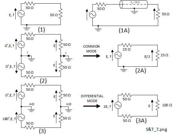
In Figure 2-1 and Figure 2-2 the direction of each of the source vector arrows represents the phase of the adjacent source at the same time instant. (1) shows the Thevenin equivalent circuit for a simple single ended 50 \(\Omega\) (one port) source, such as used on a typical VNA, correctly terminated with a 50 \(\Omega\) load. As this is unbalanced (CM), a ground symbol is included. (1A) shows how the source may be connected to the load using a coaxial cable with an impedance \(Z_0\) of 50 \(\Omega\). (2) shows how two sources, each like (1), may be combined both exactly in phase which results in the CM equivalent circuit, like (1) but with a 25 \(\Omega\) source and load impedance (2A). In (3) two sources like (1) are combined but exactly 180\( \unicode{x00B0}\)out of phase to give the balanced (DM) equivalent circuit with source and load impedances of 100 \(\Omega\) (3A). In the CM circuit (2) and the DM circuit (3) the source and load ports of the circuits may be connected using two identical \(Z_0 = 50 \Omega\) coaxial cables as shown in Figure 2-2.

In Figure 2-2 the impedance of each coaxial cable is \(Z_0\) = 50 \(\Omega \) and they are electrically identical types and lengths, so the transmission delays and the resulting phase shifts are also identical and there is therefore no differential phase caused by the cables. For (2B) the effect of the CM excitation is to connect the source impedances in parallel and the load impedances in parallel. Therefore the result is a correctly matched transmission comprising a 25 \(\Omega\) source and 25 \(\Omega\) load. However, the signal return is via the ground path so it is vulnerable to spurious CM emissions and susceptibility. For (3B) the effect of the DM excitation is to connect the source impedances in series and the load impedances in series. Therefore the result is a correctly matched transmission comprising a 100 \(\Omega\) source and 100 \(\Omega\) load. For perfect DM excitation, zero current due to the signal will flow through the ground connection. Addressing only signal transmission and not EMC, the ground connections are not actually necessary and may be omitted. In practice however, in today's harsh electromagnetic environments, screens will still be required to minimise radiated emissions and susceptibility.
Balanced and Screened Cables
Looking towards the future, a possible alternative to using two separate coaxial cables is to use a balanced transmission line designed with a standardised differential impedance between the wires. An impedance around 100 \(\Omega\) looks like a strong candidate [2] [13]. More importantly than ever, this will definitely need a screen for EMC performance. This will require to enclose the pair of DM wires as shown in Figure 2-3.

In Figure 2-3, the balanced, DM cable in (2) replaces the two separate SM cables in (1). The screen or shield totally encloses the pair of DM parallel wires. This sounds fine in theory, but the challenges come in maintaining a good shield for the DM pair at the same time as avoiding any disturbance of the integrity of the DM impedance. Traditional but high specification coaxial cables with screw type connectors provide good EMC performance. Designing a connector which is not actually coaxial, with two inner conectors, is challenging. Figure 2-4 shows the equivalent circuit for a small section of a typical DM cable.
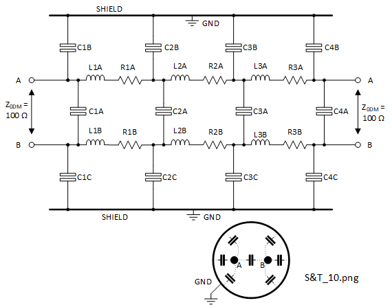
The DM wires carrying the signal are \(A\) and \(B\). Series resistance values \(R n A\) and \(R n B\) cause inherent cable loss. The remaining capacitors and inductors are designed into the cable to achieve the necessary DM impedance, ideally with no CM elements. Provided the cable is accurately excited in DM, the CM elements \(C n B \) and \(C n C \) should cause negligible 'shunting' of the DM impedance. All capacitors will include a parallel loss element which is assumed negligible (infinite values). All elements will be functions of frequency and the most significant usually result from the 'skin depth' phenomenon applied to the series resistances \(R n A\) and \(R n B\) and the series inductances \(L n A\) and \(L n B\).
Mixed Mode VNA Configurations
For the forseeable future in RF and microwave equipment, we will have to deal with CM interfaces, due to the widespread necesssity for grounded structures: ground planes, coaxial cables, convenient connectors, screening enclosures and isolation features [5]. In day to day terms this means accommodating coaxial connections to and from operating equipment and test equipment including VNAs, almost universally with 50 \(\Omega\) impedance ports. If any substantial work with mixed modes (CM and DM) is required an investment in a 4-port vector network analyzer (VNA), plus supporting hardware and software is essential [5]. Having said that, do not rule out the value of a cheaper 2-port VNA. This will provide many useful measurements but they may need some heavy processing to yield useful mixed mode information.
The 4 port VNA hardware is based upon the 2-port VNA but with more internal parts. All 4 individual ports are normally 50 \(\Omega\) impedance coaxial and therefore CM. The evolution of relative cheap and fast processing VNA capability in recent years has enabled the mathematical manipulation necessary for 4-port VNA systematic error corrections and full mixed mode \(S\) parameter measurements across large frequency ranges. The instrument calibration procedure for a 4 port VNA is more extensive than that required for its 2 port counterpart to account for the extra systematic error correction and achieving exactly the necessary CM and DM phase relationships that were described in Section 2.6. To save considerable time and to reduce errors whilst performing the calibrations, an investment in a 4 port electronic calibration (ECAL) unit is recommended.
Providing it includes all necessary hardware and software/firmware, a 4-port VNA should be capable of the following DUT measurements:
- Traditional, non-mixed mode 50 \(\Omega\) CM \(S\) parameters, DUTs 1-port up to 4-port in one operation. Any number of ports for more operations.
- 1-port and 2-port mixed mode measurements with: \(Z_0 = 25 \, \Omega \) for CM and \(Z_0 = 100 \, \Omega \) for DM, DUTs 1-port and 2-port.
We will look at ways of characterising (measuring the \(S\) parameters of) a range of DUTs across frequency which are shown schematically in Figure 2-5. We will assume access to a 4 port VNA with installed \(S\) parameter software for traditional plus mixed mode measurements, a 4 port ECAL unit and the necessary cables and adaptors..

In Figure 2-5, all coaxial cable symbols refer to 'traditional' 50 \(\Omega\) coaxial cable (CM only) connections to the VNA or other test equipment. For the mixed mode (DM and CM) stimuli and responses, each port comprises 2 traditional connections with impedances of 100 \(\Omega\) and 25 \(\Omega\) respectively. Use of an electronic calibration (ECAL) unit is highly recommended for speed, accuracy and reduction of errors. The following paragraphs comment on possible test configurations.
- N1. Port 1: DM/CM, Port 2: DM/CM
- N2 and N3. Identical Balanced to Unbalanced Transformers
- N4. Ports 1 to 4: CM 50 \(\Omega\).
- N5. Port 1: CM only 50 \(\Omega\). Port 2: CM/DM via single 50 \(\Omega\) legs.
- N6. Port 1: CM only 50 \(\Omega\). Port 2 CM only 50 \(\Omega\).
- N7. Port 1: CM only 50 \(\Omega\), Port 2 CM only 50 \(\Omega\), Port 3 CM only 50 \(\Omega\).
The DUT only has 2 mixed mode ports, 1 and 2. Setup and calibration are performed using the ECAL (8). Then VNA connections are made using VNA ports 1 and 2 to DUT port 1 and VNA ports 3 and 4 to DUT port 2. The mixed mode \(S\) parameter results are described by the mixed mode \(S\) parameter matrix, \(S_{MM}\), the format of which is shown in (2-1) [5].
For each element of the \(S_{MM}\) matrix, the first 2 letters of the subscript identify the applicable mode: differential mode (D) or common mode (C) and the numbers identify the ports, 1 or 2 in this case as it is a 2-port DUT. The 4 subscript characters represent: response, stimulus, response, stimulus in that order. For example, \(S_{CD12}\) represents a differential mode stimulus applied at port 2 and the common mode response measured at port 1.
A balanced to unbalanced transformer like N2 or N3 is also known as a balun. Each balun has a balanced (DM) port and an unbalanced (SM) port. A balun is simply designed to convert between balanced loads or sources and unbalanced loads or sources. The design challenge is achieving good performance, low transmission loss and good match, across a large range of frequencies. There will also be other parameters to consider such as power handling, temperature stability, size etc. Although the balun is a 2 port device (or network), it is not possible to characterise it using one set of \(S\) parameters because of the mixture of DM and SM port reference impedances and the absence of ground connections on the balanced side. A more test-friendly balun design may have been to use coaxial connectors for each of the balanced terminals to allow connection of each of them to the VNA. The unbalanced port could also be connected to the VNA. Then, a set of 3-port 50 \(\Omega\) \(S\) parameter measurements could be made. The \(S\) parameter results would require some processing to account for the impedance differences and the phase shift at the balanced port outputs.
Two near-identical baluns, say N2 and N3, may be connected back to back either using the CM port or the DM port. They may then be treated as a combined 2 port device and measured with either 50 \(\Omega\) or CM/DM \(S\) parameters.
This is simply a 4 port network with every port being single ended coaxial, CM-only, 50 \(\Omega\), so would be represented by a traditional non-mixed mode 4\(\times\) 4 \(S\) parameter matrix.
This DUT is like each of the baluns (N2 and N3) but differs in having connections to each of the CM/DM balanced legs separately via a single ended coaxial 50 \(\Omega\) connector. Again we have the problem of different \(S\) parameter measurement types (CM only and CM/DM) and impedance standards (50 \(\Omega\), 100 \(\Omega\) and 25 \(\Omega\)). The best approach for this might be to treat it like a 3 port 'black box' with nominal 50 \(\Omega\) CM only connections. That is, a traditional 3 port \(S\) parameter measurement.
This DUT is a classic 2 port single ended (coaxial unbalanced) network, therefore represented by a 2\(\times\)2 \(S\) parameter matrix. A simple 2-port measurement may be made after a suitable ECAL calibration.
This DUT is a classic 3 port single ended (coaxial unbalanced) network, therefore represented by a 3×3 \(S\) parameter matrix. A simple 2-port measurement may be made after a suitable ECAL calibration.
Power Levels
Before performing a batch of \(S\) parameter measurements, the power levels to be used in the measurement system require planning. We will assume that we wish to characterise a 2 port device under test (DUT) by setting up and calibrating the system for full 2 port measurements. It is not usually worth the small time saving involved in choosing subset measurement options such as 'one path 2 port', which are available on some VNAs. Any unwanted measurements can easily be ignored. However, experience has shown that 'bonus' information often highlights potential issues early which would otherwise be missed until later in the project. Using internal VNA switching, full 2 port measurements will alternately apply power to port 1 and port 2 of the VNA and therefore the asscoiated DUT ports. When power is applied to port 1 the response is measured at port 2 and vice versa.
The \(S\) parameters of a DUT are defined for linear conditions. VNAs include sensitivity controls at each port to bring incident powers from the DUT within the optimum measurement window for the instrument. When sending power (in stimulus mode) adjustable internal amplification and attenuation allows control over the power exiting the VNA towards the DUT in both directions. Some of the challenges associated power levels are summarised in the following points.
- The VNA damage threshold incident powers, including a few \(dB\) margin at both ports, must not be exceeded.
- Allowance must be made for the DUT suffering unintented instability (oscillation).
- The DUT incident power should be comfortably within its linear region, not close to either saturation or noise threshold.
- The DUT should be set up in the required operating mode and thermally stabilised before the measurement.
- The VNA IF bandwidth should be reduced as much as possible to minimise the noise floor whilst not extending the measurement time excessively.
- High values of gain or attenuation between the VNA and the DUT should be avoided as these reduce the accuracy of the result after de-embedding.
To meet these requirements, extra amplification and/or attenuation may be necessary between the VNA and the DUT, at the input, output or both. We will refer to these as external amplification or attenuation. The effects of these may be removed after the measurements by de-embedding procedures. These normally involve transmission (\(T\)) parameters, which have some limitations, and are described in Section 3. It is straightforward to reduce power levels using external attenuation. VNA output power levels may readily be reduced using the internal controls so suitably rated external attenuation is usually required to protect the VNA inputs from high DUT output power levels. Well designed attenuators behave reasonably linearly and have good reciprocity, but they contain resistive loss elements which are potential Gaussian noise sources, more apparent at small signal powers. Therefore external attenuation may be required for protection. Modern VNA have substantial output power capability, typically more than +10 \(dBm\). Should this be insufficient, external amplification may be required to drive some DUTs, for example, a high power amplifier. Unlike attenuators, amplifiers are usually designed to be highly non-reciprocal in terms of the forward and reverse transmission \(S\) parameters (\(S_{21}\) and \(S_{12}\) respectively). The reverse isolation should be very small related to the forward transmission. This may also introduce errors during de-embedding.
One option might be to use use de-embedding, usually with transmission or \(T\) parameters instead of \(S\) parameters. \(T\) parameters are described by matrices just like \(S\) parameters, and there are established formulas to convert between \(S\) parameters and \(T\) parameters in either direction. The formulas are mathematically rigorous but generally do not account for the additive white Gaussian noise (AWGN) effects of attenuators. Trying to de-embed a 40 attenuator for example will give a noise-free result which does not exist in practice. To summarise, it is certainly possible to add external components, typically amplifiers or attenuators, in order to measure a particular DUT. However, the effects of these must be de-embedded in some way which may not be straightforward and may introduce inaccuracies or noise.
Why Do You Talk About Spatial Phase? Is It Not Just Phase?
To avoid any misunderstanding I explicitly referred to spatial (space related) phase to distuinguish it from temporal (time related) phase. There is a tendancy for some to just use the word 'phase' for whatever type of phase they happen to be working on at the time. So in our case we are mainly working on spatial phase so if I forget to use the adjective 'spatial' I am probably still talking about spatial phase. A third type of phase might be instantaneous phase, the sum of temporal phase and spatial phase. Let \(\theta\) be temporal phase and \(\phi\) be spatial phase (all phase values in radians). In (2-2), \( \theta \) and \( \phi \) are the temporal and spatial phase shifts respectively.
As an example, in (1-3) we met the equations for the voltages and currents caused by a standing wave on a mismatched transmission line. Consider the forward instaneous voltage-time wave \(V_F\), by convention travelling from left to right. We are considering only one frequency at the source from, for example, a signal generator which is sinusoidal. By a convention which will become very clear, we will actually describe it by the cosine function rather than the sine function. The cosine function is of course the same as the sine function with an added phase shift of \(\pi /2 \) radian. The instantaneous voltage of a forward travelling wave \(V_F\), may be described by its trigonometric form in (2-2).
The symbols used are as follows:
- \(\theta\): temporal phase, radian (\(rad\)).
- \(\phi\): spatial phase, radian (\(rad\)).
- \(\omega\): angular frequency of the signal source, radian per second (\(rad / s\)).
- \( t \): time in seconds (\(s\)).
- \(\beta = 2 \pi / \lambda \): spatial phase constant, radian per metre (\(rad / m\)).
- \( z \): distance in the positive direction, left to right, starting at \(t = 0\), metre (\( m \)).
- \(V_F\): instantaneous voltage of the voltage time-waveform, volts (\(V\)).
- \(V_{F0}\): the amplitude or peak value of the voltage-time waveform, volts (\(V\)).
In (2-2), the negative sign before the \(\beta\) symbol is because we have chosen the positive direction along the \(z\) axis from left to right, whereas the convention for positive angle vector rotation is counter-clockwise.
From elementary trigonometry, the relationship for converting the cosine function to the sine function with a phase shift \( \pi / 2 \) radians is (2-3). Therefore, if we wished to use the sine function instead of the cosine function we would need to subtract \( \pi / 2 \) radians from the argument.
The use of exponential notation in electrical engineering is often recommended. Here is no exception. This uses Euler's well known equation for the conversion between trigonometric equations and complex exponential functions (2-4).
Using exponential notation instead of trigonometrical notation simplifies the mathematical manipulation and tends to be less error-prone. Also, it is common in electrical engineering to omit the real part operator \(Re()\) as a convenience when using exponential notation. Physical hardware can only represent real data and the imaginary coefficients are literally used only to simplify the mathematics. Using the result from (2-2) and (2-4) and omitting the \(Re()\) operator, (2-5) results.
From (2-5) it can be seen that, in exponential form, the equation for the voltage time waveform \(V_F\) has a coefficient of \( e ^{j \omega t} \) which solely is a function of the signal frequency and time. Normal VNA architecture performs the necessary measurements one frequency at a time, even if the instrument has been set up to measure across a range of frequencies. For each of these frequencies, \( e ^{j \omega t} \) is a constant factor in all of the equations and cancels out to leave just the spatial phase part, in this case \(e^{- j \beta z } \).
How Would I Characterise, Say, a 4 Port DUT Using a 2 Port VNA?
VNAs may be built with many ports but: 2 port types are common, 4 port types are less common and I have not seen one with more than 4 ports. However, we will see shortly that 4 port VNAs are useful for measuring mixed mode \(S\) parameters.
If we wish to measure the \(S\) parameters of a DUT which has more ports than the VNA we have available, we may choose either of the following methods.
- Perform multiple measurements, 2 ports at a time, each with the DUT unused ports terminated in low VSWR loads and then process the results to allocate the correct \(S\) parameter indices related to the port numbers.
- Use various switching arrangements to perform the measurements, de-embed the effects of the switches and extra cables and then process the results to allocate the correct \(S\) parameter indices.
Each of these methods is a compromise and requires an analysis of the proposed test method to determine whether it will produce final results with acceptable uncertainties.
As an example, consider that we wish to measure the \(S\) parameters of a 4 port DUT using a 2 port VNA. We will assume that the VNA has ports numbered 1 and 2, and the DUT has ports numbered 1, 2, 3 and 4. The test equipment configurations to achieve this are shown in Figure 2-6.

We could achieve this with the following steps.
- Design the test configuration using the best possible precision test cables of minimum lengths (A and B in Figure 2-6) and the fewest possible adapters.
- Procure high quality, low VSWR, broadband loads for the unused ports of the DUT with return loss values at least 10 \(dB\) greater than the best value it is required to measure at the DUT ports. These are labelled \(Z_0\) in Figure 2-6.
- Power up and allow the DUT and VNA to stabilise. Choose parameters including frequency range, incident power levels, IF bandwidth (which sets the noise floor), number of points and smoothing.
- Set up and calibrate the VNA, including cables and adapters. If possible, use an electronic calibration unit (ECAL) in preference to a manual (mechanical) calibration kit, as shown in Figure 2-6.
- Connect the VNA and DUT and loads as shown in diagram (1) in Figure 2-6 and perform the first \(S\) parameter measurement.
- Save the results electronically to a file, typically a 'Touchstone' 2 port (.s2p) file, with a unique filename which is traceable to this measurement.
- Similarly repeat measurements for each of the other configurations (2) to (6) shown in Figure 2-6, saving each set of results for later processing. Perform these measurements as quickly as possible under stable conditions.
The output of this procedure will be a set of 6 'Touchstone .s2p' files exported from the VNA. These are industry standard text files which may be readily edited or imported into applications such as Excel®, Matlab® or ADS® and processed as required. The final \(S\) parameter output data for the 4 port DUT in Touchstone format will be a .s4p file representing a \(4 \times 4 \) \(S\) parameter matrix for each frequency. This test method inevitably causes some duplication of measurements. For example, measurements (1), (2) and (4) in Figure 2-6 will each provide theoretically identical data for the DUT reflection at port 1 \(S_{11}\). There may be some small differences due to imperfect repeatability between measurements.
Figure 2-7 represents the transmission signal flow paths internal to the 4 port DUT, via each of its ports 1 to 4, which are represented by its \(S\) parameter matrix. [9] [19]

What Are \(T\) Parameters and How Might They Be Useful?
The \(S\) parameter matrix for a 2 port network with the ports numbered 1 and 2 is symbolically defined in (3-1).
Alternatively, for the same network, we could have defined the transmission (\(T\)) parameter matrix (3-2) [4].
\(T\) parameters are useful for the analysis of circuit architectures comprising cascaded networks [10] [11][12]. It is straightforward to convert between \(S\) and \(T\) parameters using matrix equations and the rules of linear algebra. Every \(T\) parameter element is a linear complex number just like those used in \(S\) parameters. Each is the intermediate result of a mathematical method and does not represent, by itself, meaningful data, unlike \(S\) parameters. The \(S\) to \(T\) and the \(T\) to \(S\) conversion formulas for 2 port networks are shown in (3-3) and (3-4) respectively [4].
One of the reasons why \(S\) parameters are so useful is that the \(S\) parameter matrix includes elements which may be easily converted to properties often used in RF and microwave engineering such as reflection coefficient, VSWR, return loss, gain and reverse isolation. Often however we require to analyse two or more 2 port networks cascaded together, such as those shown schematically in Figure 3-1. Note that, where a symbol is enclosed in round brackets, such as \(\left( S_A \right) \), this refers to the whole matrix including its elements, a total of 4 in this case as they are 2 port devices (\(2 \times 2 \)). Symbols with numeric subscripts 1 or 2, such as \(S_{11}\) or \(S_{21}\), refer to the complex value elements within each matrix.

Suppose the networks A and B, respectively in the direction of the signal flow, are cascaded together as shown in (1) where \(S_A\) and \(S_B\) are their respective \(S\) parameter matrices. This cascade is equivalent to a single 2 port network with \(S\) parameters \(S_{AB}\).
This type of configuration often occurs where the VNA does not have immediate access to all of the networks that require measuring. There may be additional cables, attenuators or amplifiers to account for. We may know the \(S\) parameters of the whole cascade \(S_{AB}\) and one of the networks, \(S_A\) or \(S_B\), and require the \(S\) parameters of the other. Alternatively we may know \(S_A\) and \(S_B\) and require \(S_{AB}\). These situations are where \(T\) parameters are useful.
\(S\) and other parameter matrices including \(T\) parameters obey the rules of linear (matrix) algebra and representing the matrix elements as complex numbers to describe magnitude and phase is compliant with these. These include keeping the correct matrix multiplication order. We can use these to help us analyse this configuration.
Performing a matrix multiplication of \(S_A\) and \(S_B\) will give us an apparently plausible result but unfortunately not what we are looking for, \(S_{AB}\). However, this procedure does work if we had used \(T\) parameters instead as shown in Figure 3-1 [2]. As we can easily convert between \(S\) and \(T\) parameters, we may use the following procedure to find \(S_{AB}\).
- Using a VNA, measure \(S_A\) and \(S_B\) separately.
- Convert \(S_A\) and \(S_B\) to their respective \(T\) parameter matrices \(T_A\) and \(T_B\) using (3-3).
- Multiply \(T_A\) by \(T_B\) in that order by applying the rules of matrix multiplication to obtain the result \(T_{AB}\).
- Convert \(T_{AB}\) to the \(S\) parameter equivalent,\(S_{AB}\) using (3-4).
For most networks, especially active devices, there will be one \(S\) parameter matrix for each set of fixed conditions such as frequency, temperature and DC voltage. So, for a typical measurement session, many such conversion calculations like those we have discussed will be required.
Taking this a stage further, a very common requirement is to measure the \(S\) parameters of a device (DUT) at a range of ambient temperatures which deviate from normal room temperature. The DUT needs to be installed in a thermal chamber, powered up and then its \(S\) parameter performance measured across a range of temperatures as required. The VNA would normally be positioned external to the chamber but close to it and the connections to the DUT made via relatively long cables passing through suitable insulated chamber apertures. Other cables necessary for the DUT operation would be similarly routed via apertures. Such a configuration would effectively comprise 3 cascaded 2 port devices as a whole connected to the VNA: the input cables, the DUT and the output cables. We will name the associated \(S\) parameters \(S_A\),\(S_B\) and \(S_C\) respectively. These are shown schematically with associated matrix equations in Figure 3-2.

As with the simpler 2 network cascade, we cannot readily remove or de-embed the effects of the input and output cables using their \(S\) parameters directly. Initially, we need to measure the \(S\) parameters of the input and output cables separately and then convert each set of these measurements to \(T\) parameters using the \(S/T\) conversion equations (3-3) and (3-4). Referring to Figure 3-2 this procedure would provide \(T\) parameters \(T_A\) and \(T_C\) for the input and output cables respectively. Then the \(S\) parameters of the whole cascade \(S_{ABC}\) would be measured and also converted to \(T\) parameters to give \(T_{ABC}\). Using the rules of linear algebra for matrix equations the \(T\) parameters of the DUT \(T_B\) may then be calculated using the expression for \(T_B\) which is included in (3-5). This may be converted back to the corresponding \(S\) parameters using the conversion equation (3-4).
How Would I Extract Group Delay Data from \(S\) parameter Matrices?
We will assume 2 port networks with ports 1 and 2 being the input and output respectively, so \(S_{21} \) is the (linear transmission) gain and phase. Group delay (\( \tau \)) is defined as the \(S_{21} \) rate of change of phase with respect to frequency with a coefficient of -1 (4-1).
Where:
- \(\phi \): spatial phase, radian (\(rad\)).
- \(\theta \): spatial phase, degrees (\(\unicode{x00B0}\)).
- \(\omega \): angular frequency, radian per second (\(rad/s\)).
- \(f \): frequency, hertz (Hz).
The group delay equations are shown for transmission (\( S_{21} \)) phase angles in both radians and degrees. The adjective 'group' in group delay means that its calculation is across a small 'group' of frequencies with respect to the absolute frequency \(f\). This is consistent with the \({d \phi} / { d \omega } \) term in the differential equation so the accuracy of the result will be increased for larger numbers of measurement points. Example plots of \( S_{21} \) phase against frequency are shown in Figure 4-1 for a high specification, dispersion free, solid dielectric coaxial cable; in Figure 4-2 and Figure 4-3 for an untuned bandpass filter (BPF) log magnitude and phase and in Figure 4-4 for the same BPF but group delay (\(\tau\)). For both the frequency range is 50 \(MHz\) to 150 \(MHz\). As (4-1) implies, the group delay is derived from the gradient of phase against frequency. The cable is working well within its frequency specification so the group delay is constant across the whole range. However, the BPF phase response is highly non-linear due to the delay distortion introduced by the BPF reactive elements.

The coaxial cable length is 1 \(m\) and the relative permittivity of the dielectric material, \(\epsilon_r \) is 2.1. The transmission phase response is 'unwrapped' for clarity. Most VNAs default to display 'wrapped' phase which can readily be 'unwrapped' if required. However, the accuracy of unwrapped phase degrades with higher frequencies and longer cables which therefore 'contain' many wavelengths.
The phase frequency slope of the cable should remain constant down to zero frequency. This may be verified by extrapolating Figure 4-1 to DC. The slope is approximately 1.73 \(\unicode{x00B0} / MHz\). Substituting this value into (4-1) and doing the necessary unit conversions yields a group delay of \(\tau = 4.8 \, ns\). In this case the group delay is constant across frequency and equivalent to the absolute delay of the cable. To verify this, the propagation velocity through the cable would be \(c / \sqrt{\epsilon_r} = 2.07 \times 10^8 \, m/s \). The length is \( 1 \, m \) so the absolute delay is \( 1 / (2.07 \times 10^8) \, m/s = \, 4.8 \, ns \).

The BPF results shown in Figure 4-2, Figure 4-3 and Figure 4-4 was designed aiming at an Elliptic architecture so the poles and zeros were formed using series and parallel resonant circuits. The reactive components used for resonant circuits cause all sorts of interesting phenomena.

In the passband range of approximately \( 60 \, MHz \) to \( 80 \, MHz \) the phase frequency slope is fairly constant at about \( 13.1 \unicode{x00B0} \, / MHz \). By again substituting this into (4-1) and doing the necessary unit conversions the group delay around these frequencies comes to about \( 36.4 \, ns \). Figure 4-4 shows a group delay against frequency plot of the same filter.
