Introduction
This article discusses the properties of real, passive, lumped element components: inductors, capacitors and resistors, which are designed to operate at what we will describe as RF and microwave frequencies. Most of the discussion is with nominally reactive parts (inductors and capacitors) but resistors are also included. That is because each type of real lumped element component will exhibit some secondary characteristics of the other two types. Inductors will have elements of capacitance and resistance; capacitors will have elements of inductance and resistance and resistors will have elements of inductance and capacitance. Well designed components will have very small components of secondary characteristics and these may have negligible reactances at low frequencies compared to those of the intended component. However, as the operating frequencies are increased, the effects of the secondary characteristics become more and more significant and start to seriously degrade the electrical performance. We will look at some of these with examples.
System International (SI) Units
The units used in this article for the electrical parameters are derived from Systeme International (SI) Units and are summarised in Table 1-1. The short-form SI unit symbols, such as farad (\(F\)) for capacitance, ampere (\(A\)) for electric current and ohm (\(\Omega\)) for impedance, are derived from the SI Base Units: mass (kilogram, \(kg\)), length (metre, \(m\)), time (second, \(s\)) and electric current (ampere, \(A\)). It is usually less cumbersome to use the short-form symbols. It is also common practice, where appropriate, to use metric multiplication factors with the SI Base Unit symbols. These are summarized in Table 1-2
| Parameter | SI Derived Unit(s) | SI Base Unit(s) | ||
|---|---|---|---|---|
| Name | Symbol | Name | Symbol | |
| Capacitance | \(C\) | farad | \(F\) | \( kg^{-1} \, m^{-2} \, s^{4} \, A^{2} \, \) |
| Inductance | \(L\) | henry | \(H\) | \( kg^{} \, m^{2} \, s^{-2} \, A^{-2} \, \) |
| Voltage | \(V\) | volt | \(V\) | \( kg^{} \, m^{2} \, s^{-3} \, A^{-1} \, \) |
| Electric Current | \(I\) | ampere | \(A\) | \( A \, \) |
| Permittivity | \(\epsilon \) | farad/metre | \(F/m\) | \( kg^{-1} \, m^{-3} \, s^{4} \, A^{2} \, \) |
| Permeability | \(\mu \) | henry/metre | \(H / m \) | \( kg^{} \, m^{} \, s^{-2} \, A^{-2} \, \) |
| Time | \(t\) | second | \(s\) | \( s \) |
| Mass | \(m\) | kilogram | \(kg\) | \( kg \) |
| Length | \(l\) | metre | \(m\) | \( m \) |
| Frequency | \(f\) | hertz | \(Hz\) | \( s^{-1} \) |
| Angular Frequency | \(\omega\) | radian/second | \(rad/s\) | \( s^{-1} \, \) |
| Q-factor | \(Q\) | None | None | \( None \) |
| Power | \(P\) | watt | \(W\) | \( kg^{} \, m^{2} \, s^{-3} \, \) |
| Energy | \(U\) | joule | \(J\) | \( kg^{} \, m^{2} \, s^{-2} \, \) |
| Impedance | \(Z\) | ohm | \( \Omega\) | \( kg^{} \, m^{2} \, s^{-3} \, A^{-2} \, \) |
| Resistance | \(R\) | ohm | \( \Omega \) | \( kg^{} \, m^{2} \, s^{-3} \, A^{-2} \, \) |
| Reactance | \(X\) | ohm | \( \Omega \) | \( kg^{} \, m^{2} \, s^{-3} \, A^{-2} \, \) |
| Admittance | \(Y\) | siemen | \( S \) | \( kg^{-1} \, m^{-2} \, s^{3} \, A^{2} \, \) |
| Conductance | \( G \) | siemen | \( S \) | \( kg^{-1} \, m^{-2} \, s^{3} \, A^{2} \, \) |
| Susceptance | \( B \) | siemen | \( S \) | \( kg^{-1} \, m^{-2} \, s^{3} \, A^{2} \, \) |
Frequency Ranges
We will study the properties of lumped, passive components in circuit designs operating at radio frequencies (RF), microwave frequencies and 'high speed digital' transmission speeds. Add to the list 'wireless' frequencies, a term which has become popular again after many years. Here we are considering circuit parts that would typically be assembled (soldered) onto planar circuit boards down to a minimum size of 0402. We are not considering integrated circuit (IC) or hybrid circuit design. We will refer generally to these frequencies as 'RF and microwave' frequencies, broadly up to about 1 GHz, it being understood that full frequency range data are available from the associated datasheets and the technology is continuously improving enabling even higher operating frequencies. By 'high speed digital' we mean the greatest bit rate used on the baseband spectrum. This is normally standarised to a periodic 'clock' waveform with (theoretically) 'square' voltage-time edges. A Fourier analysis of this will yield a theoretically infinite bandwidth so this must be limited for practical circuits. Actual bandwidths are also functions of the type of waveform, such as return-to-zero (RZ) or non-return-to-zero (NRZ), the coding and baseband filtering. After accounting for these the RF design should be based upon highest frequency component of the resulting baseband spectrum plus a suitable margin to allow for temperature effects, tolerancing etc..
Lumped Element Components
Real lumped element components are designed to operate at frequencies in which the shortest wavelength in use is much greater than the order of the component dimensions. They are designed to approximate as closely as possible to ideal (perfect) versions of inductors, capacitors or resistors across the widest possible frequency range. The most up to date designs mostly use surface mount technology (SMT) with a few still using 'through hole technology'. In the real world, inductors will have elements of capacitance and resistance, capacitors will have elements of inductance and resistance and resistors will have elements of inductance and capacitance. Each of these unwanted (secondary) characteristics will usually be quite complicated functions of frequency and difficult to predict.
As with much of RF and microwave engineering, there are no hard and fast rules but the 'much less than the shortest wavelength' criterion is often understood to be less than about 10%. This is usually interpreted that the shortest wavelength must be at least ten times the maximum physical dimension of the component 'shell' under consideration, with no further modification applied. We will see that even this 'ten times rule of thumb' might not be conservative enough when we account for self-resonant frequencies (SRFs).
The following is a list of manufacturers whose products include various lumped element components which have been designed for RF and microwave frequencies. We will be using some of their datasheets and application notes. More details are included in the references [14] [15] [16] [17] [18].
- Coilcraft (mostly inductors)
- Murata (mostly capacitors)
- Kemet (capacitors and inductors)
- TDK (capacitors and inductors)
- AVX (capacitors, inductors and resistors)
- Vishay (capacitors and resistors)
- Johanson Technology (capacitors and inductors)
- Bourns (resistors)
To get some realistic examples we will overview a few example products.
Lumped Element Inductors
The lumped element inductor designs being considered are essentially just small coils with or without magnetic cores. Earlier designs would have helically wound copper wire coils with the ends unterminated to enable trimming and soldering to the circuit as required. The more recent surface mount technology (SMT) has dictated profiles appropriate to mounting on high frequency planar circuits such as microstrip.
Predicting and measuring high frequency performance of lumped element inductors is usually more challenging than the equivalent exercise performed for capacitors or resistors. That is because the inductor designs are more complicated and have less predictable parameters. Some of those to be considered are listed below [3] [4] [5] [10].
- Coil: dimensions, wire gauge and type (resistive losses, power handling).
- Turn spacing (affects interwinding capacitance).
- Wire AC resistance (skin effect, proximity effect).
- Self resonant frequencies and Q-factor (unpredictable functions of frequency).
- Core magnetic properties (suitably high frequency materials must be used).
- RF and DC voltage and current handling.
- RF and DC power dissipation.
For example, the Coilcraft® part 2222SQ-90N is a 90 nH air core surface mount inductor with approximate dimensions 5.2 mm \(\times\)5.5 mm \(\times\) 5.7 mm, so the maximum dimension of the component shell is 5.7 mm [15]. Suppose that this was used on a 50 Ω microstrip circuit on FR4 substrate with an effective dielectric constant, \(k_{eff}\) of 3.5. Some graphs from the Coilcraft datasheet in Figure 1-1 for this component show that its measured Q-factor and nominal inductance are reasonably predictable up to about 200 MHz before the curves get distorted.

For operation above 200 MHz, say up to about 500 MHz, if we were expecting some reasonably well-behaved inductive behavoir close to 90 nH we would be disappointed. Also look at the Q-factor at 500 MHz, which is taking off quite rapidly. Is that not what we need? Probably not. The strange behavoir of the curves is caused by parasitic resonances, or self resonant frequencies (SRFs). SRFs are caused by various series and parallel resonances exploiting small elements of inductance and capacitance inherent in the physical design of the component. Sometimes these can happen to be useful for what we are trying to electrically achieve, such as a high impedance properties we expect to get from inductors used as RF blocking 'chokes'. However, choke applications need a different design approach. Here we are looking for inductors as close to ideal as possible such as might be required in a filter. Most inductor manufacturers include ranges for 'chokes' separately from 'conventional' use such as filter design.
The shortest wavelength, at 200 MHz, is 1.5 m in air. For the suggested FR4 microstrip transmission line, this reduces to \(1 / \sqrt{ k_{eff}} \) times the air wavelength in the microstrip medium, which is 0.83 m. So in this case the longest dimension of the component is actually about 0.007 of a wavelength. If we desired to use the part at 500 MHz in the same microstrip circuit, that would be a wavelength within the FR4 material of about 0.32 m, still well within our 'less than one tenth of a wavelength' criterion. However, we would then have additional challenges from the SRF issues. In conclusion, the 'less than one tenth of a wavelength' criterion in most cases is insufficient to avoid SRF issues.
Lumped Element Capacitors
With few exceptions, lumped element capacitors are designed for use in SMT form again probably with microstrip architecture still being the most popular. RF and microwave performance is generally more predictable and Q-factors are higher for similar frequency ranges, assuming approximately the same reactance magnitudes compared to lumped element inductors. However, they still exhibit self resonant characteristics as the operating frequencies are increased.
The following list applies to lumped element characteristics applicable to capacitors. All parameters are functions of frequency.
- Q-factor and self resonance frequencies.
- Series and/or parallel equivalent loss resistances.
- Dielectric material: dielectric constant and loss tangent.
- AC and DC handling: voltage, current and power dissipation and breakdown.
Products from Johanson Technology® include the 'S-Series' range of High-Q multi-layer surface mount capacitors [16]. Some typical parameters for the 0603 R14S high-Q range are shown in Figure 1-2, Figure 1-3, Figure 1-4 and Figure 1-5. Some comments on each of these are noted below.
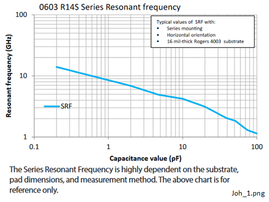
The 90 nH Coilcraft inductor we studied in Section 1.3.1 had an inductive reactive magnitude of about 113 Ω at 200 MHz. For a capacitor, the same reactive magnitude, but capactive, would require a value of about 7 pF. From Figure 1-2 the resonant frequency for this value is expected around 4.5 GHz, much greater than the operating frequencies we were considering with the inductor. Therefore, in general we expect to have more freedom with capacitor choice than inductor choice. Also capacitors for otherwise similar ratings, tend to be cheaper, so if the design allows it, it is usually better to minimise the inductor part count compared to capacitors.
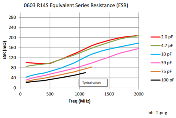
One equivalent circuit for a real capacitor comprises an ideal capacitor and resistor connected in series. The associated resistance value is known as the equivalent series resistance (ESR) or \(R_{ESR} \)which is plotted in Figure 1-3 against frequency. The Q-factor \(Q_{CS}\) relationship for this is shown in (1-1).
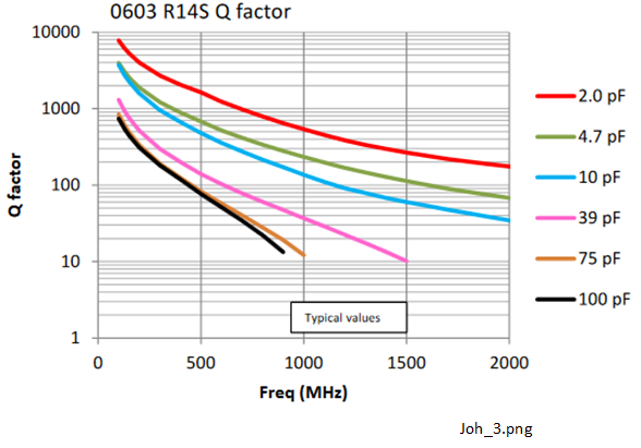
(1-1) relates \(Q_{CS}\) to \(R_{E S R}\). For example, for a 75 pF capacitor at 500 MHz, the ESR is 43 mΩ and \(Q_{CS}\) is 99. Figure 1-4 shows the \(Q_{CS}\) variation with frequency to be reasonably predictable for several of the capacitor range. This implies that there are no troublesome SRFs of the type observed with lumped element inductors.
Lumped Element Resistors
Relatively few lumped element resistors are actually used at RF and microwave frequencies, sometimes referred to as 'broadband' frequencies in the data sheets. Resistors represent a waste of power and are a source of additive white Gaussian noise (AWGN), which contributes to noise figure. Their use is generally limited to biassing, isolated loads, attenuators and broadband matching functions. The nominal resistance values available are usually limited accordingly. Q-factors are defined for reactive components only and are therefore not relevant to resistors. Resistors do exhibit some parastiic inductive and capacitive elements due to their inherent electrical properties but these are far less serious than those affecting inductors and capacitors.
Some examples of broadband resistor data are included in the product range from Kyocera-AVX in Figure 1-5 and Figure 1-6 [17].
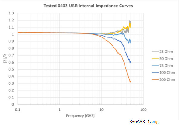
Figure 1-5 shows that the normalized impedance magnitude is close to unity up to about 6 GHz. It then diverges into both the capacitive and inductive regions by diferent paths according to the nominal value. These are caused by the parasitic behavoir, or secondary characteristics, of the capacitive and inductive elements. No measureable SRFs were visible within the frequency ranges examined for the lumped element inductors and capacitors, up to about 1 GHz. It is interesting to note that there is some small SRF behavoir apparent above about 10 GHz. In general, provided good quality broadband resistors are used, SRFs are not expected to degrade performance.

The S-parameter test results shown in Figure 1-6 for the 25 Ω resistor indicate that the system impedance is also 25 Ω instead of the more common 50 Ω or 75 Ω. Therefore the source and load reference impedances were both 25 Ω and the \(S_{21}\) and \(S_{11}\) plots agree with the S-parameter predictions for near-ideal resistors at frequencies well above 1 GHz. The S-parameter results for the other nominal resistor values (not shown) were almost identical.
Q-Factor, Self Resonant Frequencies and Loss Tangent
Q-factor (colloquially known as 'quality factor'), self resonant frequency (SRF) and loss tangent (alternatively tan delta, tanδ or dissipation factor) are parameters which describe how well various passive reactive components and resonant circuits perform as functions of frequency. In RF and microwave design we need to consider frequency spectra extending perhaps into several gigahertz. As frequencies extend upwards, the electrical behaviour of passive components depart significantly from what we would have expected, if we had assumed them to be ideal.
There are many manufacturers of lumped element capacitors and inductors but many are designed for high volume and low-cost. These result in inferior specifications which may be adequate for low frequencies such as those used in switched mode power supplies. Far fewer manufacturers have invested in developing high-Q versions of these for targeting RF and microwave frequencies. High-Q performance represents added value so we can expect to pay more for these.
Q-Factor Overview
Contrary to some people's understanding, including my own, the concept of Q factor was never originally suggested to represent 'quality' factor, despite the fact that this is precisely what it does represent to users of the English language. It just happened to be a letter left over after the others had been used as symbols for other parameters [8] [9].
There are essentially two definitions of Q-factor, as follows [2] [6]:
- Single lumped element reactive components with no intended self-resonant behaviour as a function of frequency.
- Intentionally designed resonant circuits: those including at least one capacitor and one inductor, to show the 'sharpness of resonance' as a function of frequency.
In the first case, Q-factor is a measure of how closely the electrical performance of the reactive component compares to an ideal version of the same component at the nominal value over a range of frequencies. Usually, the most predictable behaviour will be in regions of the Q-factor function well below any apparent self resonant frequencies (SRFs). Any SRFs which may exist are in general unwanted and they should be avoided [6]
In the design of resonant or tuned circuits, Q-factor is a measure of the 'sharpness' of the resonance in terms of voltage or current amplitudes within the circuit across a range of frequencies. In this case, there is one Q-factor value for each circuit and loading condition and, again, a higher Q-factor represents a closer to ideal performance or a sharper response. In these cases Q-factors may be unloaded or loaded. Unloaded Q-factors are a useful theoretical concept and consider the resonant circuit completely in isolation, so the spread of Q-factor values against frequency will be fixed. In the real world however, resonant circuits require to be coupled to other circuits and therefore become 'loaded'. Loaded Q-factors are also expressed as functions of frequency but take into account the explicit loading of the resonant circuit. Unloaded Q-factors are always greater than loaded Q-factors.
Later, when we examine the circuit currents and voltages over higher and higher frequencies, we will see some anomalous behaviours which are caused by phenomena known as skin effect and proximity effect [1]. These affect both the resistance and inductance parameters and are always functions of frequency. Others are SRFs. These are caused by the resonant effects of inherent stray capacitances and inductances both with other strays and with the intended bulk capacitance or inductance. In general, the challenges of dealing with strays and SRFs are greater with inductors than with capacitors. Even for well designed, high frequency components there will typically be a few series or parallel SRFs present. These should be avoided by choosing parts in which the lowest SRF is well above the maximum operating frequency.
Sometimes, SRFs may happen to be useful if for example they help to reject a narrow band of unwanted spurious frequencies. However, for these type of problems a better targeted solution should be found because the positions and behaviours of SRFs were never intended and may not be consistent or repeatable after allowing for the full operating conditions including temperature.
Q Factor for Lumped Components at Low Frequencies
Firstly, we will look at the Q-factors of real capacitors and inductors at relatively low frequencies: those are frequencies at which they may be accurately considered as a simple network of perfectly reactive or resistive components. For each case, the equivalent circuit of the real component may be considered either as a series or parallel combination of an ideal capacitor (or inductor) and an ideal resistor. The circuit schematics, phasor diagrams and derived Q-factor formulas for these are shown in Figure 2-1 and Figure 2-2 for capacitors and inductors respectively.


In each of the equivalent circuits, the Q-factor symbol '\(Q\)' is subscripted '\(C\)' for the capacitor or '\(L\)' for the inductor followed by either '\(S\)' for series equivalent circuit or '\(P\)' for parallel equivalent circuit. Lower case omega (\(\omega\)) represents the angular frequency in radians per second (\(rad / s\)), so \(\omega = 2 \pi f\), where \(f\) is the frequency in hertz (\(Hz\)). For these ideal components, the inductor voltage phasor leads its current by exactly \(\pi / 2\) radians and the capacitor voltage phasor lags its current by exactly \(\pi / 2\) radians.
Refering to the equivalent circuits for the real capacitor in Figure 2-1, an ideal capacitor dielectric is theoretically a perfect insulator. The relative permittivity (or dielectric constant) of the dielectric material also contributes the capacitance value itself: the greater the relative permittivity, the greater is the capacitance that can be achieved in a fixed space envelope. Design engineers are usually pressured to reduce the size of components, for capacitors perhaps choosing parts with greater dielectric constant. Unfortunately, this typically degrades the Q-factor, creating a less than perfect insulator, one with a finite resistance and therefore reduced Q-factor. In Figure 2-1 the leakage resistance is represented equivalently, either by a high value in parallel or a low value in series with the ideal capacitor, \(R_{CP}\) and \(R_{CS}\) respectively. Derived from the magnitudes of the voltage and current phasors shown in Figure 2-1 the Q-factor expressions for the series and parallel CR equivalent circuits are given by (2-1) and (2-2) respectively.
In Figure 2-2, the equivalent circuits for real inductors are also represented by resistance values in series (\(R_{LS}\)) or in parallel (\(R_{LP}\)) with the ideal inductance element. A significant contribution to (\(R_{LS}\)) usually comes from the resistance of the wire used to construct the inductor coil. The Q-factor expressions for the series and parallel LR equivalent circuits are given by (2-3) and (2-4) respectively.
As we noted in Section 1.3.1, several manufacturers promote ranges of high-Q lumped element inductors and capacitors. For example, data sheets by Coilcraft® typically include graphs of Q-factor and deviation from the nominal values, both against frequency. One example, shown in Figure 2-3, is extracted from their datasheet for the product parts 1515SQ, 2222SQ and 2929SQ, covering nominal values from 47 nH to 500 nH. The datasheet confirms that these are indeed measured results and, importantly, Coilcraft also provides supporting information including how they were measured with details of test equipment, test jigs and calibration methods. Reliable and measured data like this are essential for rapid and effective RF and microwave circuit design.
In Table 2-1 for the Coilcraft 1515SQ 90 nH inductor, at several frequencies I have calculated the values of equivalent circuit series resistance (\(R_{LS}\)) and parallel resistance (\(R_{LP}\)) with values of Q and frequency taken from the datasheet, using (2-3) and (2-4) respectively.
| Frequency (\(MHz\)) | Q-factor | \(R_{LS}\) (\(\Omega\)) | \(R_{LP}\) (\(\Omega\)) |
|---|---|---|---|
| 1.0 | 40 | 0.014 | 0.023 |
| 5.0 | 65 | 0.043 | 0.184 |
| 10.0 | 80 | 0.071 | 0.452 |
| 20.0 | 115 | 0.098 | 1.301 |
| 50.0 | 170 | 0.166 | 4.807 |
| 100.0 | 215 | 0.263 | 12.158 |
The datasheet reports that the DC resistance of the 90 nH inductor (equivalent to \(R_{LS}\) at zero frequency) is 0.0055Ω. As the frequency is increased however, it is clear that the actual value of \(R_{LS}\) also increases in some, as yet unknown, function of frequency. So even in well designed, high-Q, real inductors we cannot make any assumptions about constant coil resistance if we need to accurately measure their RF characteristics. This increase in resistance with frequency is probably caused by the skin effect acting on the copper wire used to construct the inductor coil [1] [4]. The skin effect forces the AC current to pass through a thin layer on the surface of the wire which forms the inductor and its thickness reduces with increasing frequency. There may also have been a contribution from a phenomenon known as proximity effect. Proximity effect is caused when adjacent turns of an inductor coil are so close that the current distribution in one turn influences that in the next. This also increases with frequency but is not as predictable as the skin effect. Increasing the turn spacing does tend to reduce this but this practice also affects other parameters and may increase the dimensions. Even with these limitations, we can see from Figure 2-3 and (2-3) that there is a net and predictable increase in Q-factor for the 90 nH inductor from 1 MHz up to about 200 MHz.
Returning to Figure 2-3, the left plots of Q-factor against frequency all come to peaks towards the high frequency ends. In the plots of the inductance values against frequency on the right, it is clear that the actual inductance values are close to their nominal values for most of the frequency range and then start increasing, broadly at similar frequencies. These again are likely to be the effects of SRFs.
Some examples of high frequency data for high Q capacitors from the Murata® GJM range are shown in Figure 2-4. Although this example is for a nominal value of 4.7 pF, it is representative of the whole GJM range.

The plots on the left are of equivalent series resistance (ESR) for the capacitor against frequency. This parameter is often used for capacitor specifications and is equivalent to \(R_{CS}\) which was used in Figure 2-1 and (2-1).
In general, for high-Q lumped components, assuming similar frequencies and reactance magnitudes, capacitors tend to have better Q-factor performance than inductors. This is due to the architecture of the lumped element inductor having much more scope for parasitic effects (secondary properties) than the lumped element capacitor. Therefore, if a circuit design allows the option of using one or more capacitors instead of an inductor, this may improve the higher frequency performance.
The ESR and Q-factor plots in Figure 2-4 may be related to each other using the equation for \(Q_{CS}\) (2-1) or \(Q_{CP}\) (2-2). For example, with the 'new material' GJM part, measured Q-factors were 500 and 230 at 500 MHz and 1000 MHz respectively. Using (2-2), the respective calculated \(R_{CS}\) are 0.14 Ω and 0.15 Ω.
Unloaded Resonant Circuits
Q-factor may be used to describe the sharpness of resonance of real resonant circuits or tuned circuits [2]. There are two simple types of resonant inductor-capacitor (LC) circuits: series and parallel. Schematics of the ideal versions of these are shown in Figure 2-5 (a) and Figure 2-6 (a) respectively.
In both cases the (angular) frequency (\(\omega_{0}\)) is given by (2-5):
For reference, Table 2-2 provides the standard formulas for impedance (\(Z\)) and admittance (\(Y\)) of the ideal circuit elements inductance, capacitance and resistance.
| L (henry, \(H\)) | C (farad, \(F\)) | R (ohm, \(\Omega\)) | |
|---|---|---|---|
| \[Z (\Omega)\] | \[j \omega L \] | \[ \frac{-j}{\omega C} \] | \[R\] |
| \[Y (S)\] | \[ \frac{-j}{\omega L} \] | \[j \omega C \] | \[ \frac{1}{R} \] |
In Figure 2-5 (a) and Figure 2-6 (a), no resistance or Q-factor information for \(L\) nor \(C\) is shown. The implication of this is that the Q-factors of both circuits are infinite. This implies that the equivalent series resistances for \(L\) and \(C\) are both zero. Alternatively, the equivalent parallel resistances for \(L\) and \(C\) are both infinite. Unfortunately this would not be any use other than as a theoretical concept because neither circuit is connected to anything. Neither circuit would actually be practical or actually have a resonant frequency. More precisely, both circuits would have a resonant frequency but it would occupy zero bandwidth.
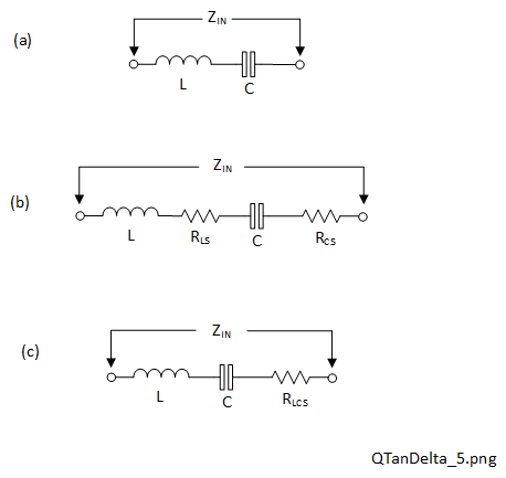
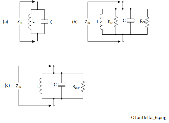
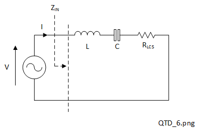
A more practical resonant circuit, one of which is shown in Figure 2-5 (b) was derived from Figure 2-5(a) but with series resistances \(R_{LS}\) and \(R_{CS}\) added to represent the additional losses present in the inductor and capacitor respectively. It would have been just as correct to represent the additional losses by parallel loss resistances, \(R_{CP}\) and \(R_{LP}\), as shown in Figure 2-6(b) but the series versions are easier to consider for a series resonant circuit. One further simplification is shown in Figure 2-5 (c), where \(R_{LCP}\) simply represents the combined loss resistances (sum) of \(R_{LS}\) and \(R_{CS}\) in series so they are added (2-6).
The complex input impedance \(Z_{IN}\) of the circuit shown in Figure 2-5 (c) is given by (2-7):
As an example of a real series resonant circuit, consider the Coilcraft 90 nH inductor that was examined in Section 2.1.1. To choose an arbitrary resonant frequency of 100 MHz would, from (2-5) require a capacitor value of approximately 28 pF. The impedance magnitude for this circuit was plotted using Matlab 2023a® across a frequency range 90 MHz to 110 MHz. The result, normalised to 100 MHz, is shown in Figure 2-7.
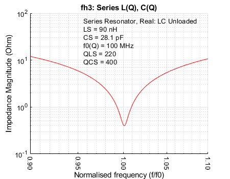
In this case we have assumed the Q-factors to be relatively constant across this small frequency range with the values of \(Q_{LS}\) =220 for the inductor and \(Q_{CS}\) = 400 for the capacitor, both measured at 100 MHz.
The impedance magnitude plot in Figure 2-7 shows the classic shape predicted in AC theory for a series resonant circuit with the resonant frequency at 100 MHz. At resonance, the impedance magnitude is at a minimum at approximately 0.4 Ω which corresponds to the impedance having no complex component and is equivalent to \(R_{LCS}\) from (2-6). This may be confirmed by calculating \(R_{LS}\) (0.26 Ω) and \(R_{CS}\) (0.14 Ω) using (2-3) and (2-1) respectively and then using these results in (2-6) to give the combined result.
For the parallel form of resonant circuit, refer to the circuit schematics shown in Figure 2-6. In this case the reactive elements and loss resistances are all connected in parallel. Then the standard reciprocal relationships between them (2-8) may be applied as required.
For the parallel resonant circuit, \(R_{LP}\) and \(R_{CP}\) may be calculated using (2-4) and (2-2) respectively, yielding the results \(R_{LP}\) = 12.441 kΩ and \(R_{CP}\) = 22.736 kΩ. The equivalent resistance \(R_{CLP}\) for both may be obtained from the parallel resistance formula (2-8) which comes to 8.041 kΩ.
The input admittance (\(Y_{IN}\)) of the parallel tuned circuit shown in Figure 2-6 (c) is given by (2-9):
For consistency with the series resonant circuit, the input admittance may be converted to input impedance using the reciprocal relationship (2-10):
After using (2-9) and (2-10) as described, Figure 2-8 is a plot of the magnitude of the input impedance for the parallel resonant circuit against frequency, created again using Matlab 2023a®.
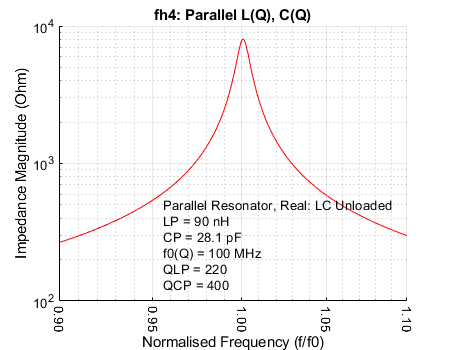
As expected, the real resistance at resonance is about 8.041 kΩ calculated using (2-8)
Complex Power and Energy
The Q-factor definition for a resonant circuit is related to energy so, to examine this in more detail, consider a real series LC resonant circuit, similar to Figure 2-5(c), which is connected directly to an AC Thevenin constant voltage source as shown in Figure 2-9 [2]
.
A resistor (\(R_{LCS}\)) has been added in series to represent the loss resistance of the inductor and capacitor combined. The input impedance is the complex quantity \(Z_{IN}\), the applied (sinusoidal) voltage and current phasors are \(V\) and \(I\) respectively. The peak values of \(V\) and \(I\) are \(V_0\) and \(I_0\) respectively. Therefore the voltage and current waveforms would be of the forms: \(V = V_0 \sin \omega t \) and \(I = I_0 \sin \left( \omega t + \phi \right) \) respectively, where \(\phi\) is an arbitrary phase angle.
In circuits like these there is no explicit source or load resistance connected as we might have expected if we were examining, for example, a 2 port network. The actual resistance shown \(R_{LCS}\) represents the equivalent series loss resistances for the inductor and capacitor combined on account of them being real components and having finite Q-factors. Ideal reactive components do not dissipate any power but they can store energy, either in the magnetic field for an inductor or in the electric field for a capacitor. A resistor can of course dissipate power but cannot store energy.
The energy stored in a capacitor (\(W_{E}\)) and in an inductor (\(W_{M}\)) are given by (2-11) and (2-12) respectively. In each case it is assumed that the energy integration time is over many cycles [2].
A sinusoidal voltage is applied to the series resonant circuit so the voltages and current within the circuit will both also be sinusoidal. The resulting energy against time functions, we can see from (2-11) and (2-12) will be sine or cosine squared, as the energies must of course be positive. The squared functions therefore also double the frequency compared to the fundamental applied by the voltage source. This implies that, the energy content transfers on alternate half cycles between the capacitor and the inductor.
The complex input power delivered to the resonator (\(P_{IN}\)) is (2-13):
In (2-13), \(I^{*}\) is the complex conjugate of \(I\).
From (2-13), the complex power comprises a real part which we will call \(P_{LOSS}\) (2-14) and an imaginary part with two components, one from the inductor and one from the capacitor.
Ideal reactive components do not dissipate any power which is consistent with \(L\) and \(C\) only being present in the imaginary coefficients. As we are in fact representing real components, defined with finite Q-factors, the power loss in each case will actually be included in \(P_{LOSS}\).
\(P_{IN}\) can also be expressed in terms of \(P_{LOSS}\) and the inductor and capacitor energies, \(W_M\) and \(W_E\) respectively. This is shown in (2-15), which comes from (2-13) using expressions for \(W_E\) and \(W_M\) from (2-11) and (2-12) respectively.
From (2-15) it is clear that the resonant condition is when the capacitive and inductive energies are identical, so \( W_M = W_E \). By substituting the associated energy equations in (2-11) and (2-12), we arrive at the resonance relationship (2-5), which is repeated here (2-16) [2].
Definition of Q-Factor for a Resonant Circuit
Q-factor is a measure of the loss of a resonant circuit and is defined in (2-17). The greater the Q-factor the smaller the loss.
Let us assume, at the resonance frequency, that \( \omega = \omega_0 \). At resonance we know that \( W_E = W_M \). Therefore, the expressions for Q-factor, in terms of each energy component are (2-18) and (2-19).
By substituting the expressions for \( W_M \) from (2-12) into (2-18) and for \(W_E \) from (2-11) into (2-19), the Q-factor equations shown in (2-20) and (2-21) may be confirmed.
To examine the behaviour of the Q-factor response curve near resonance, at an angular frequency of \( \omega \) rad/s, one may assume (2-22), where \( \Delta \omega \lt \lt \omega \).
We know from (2-5) that \( {\omega_0}^2 = 1/LC \). Furthermore, from elementary algebra (2-23).
Using (2-23) and substituting into (2-7), \(Z_{IN}\) may then be expanded to include \(\omega\), \(\omega_0\) and \(\Delta \omega\) (2-24).
From (2-13), when the frequency is such that \( {\mid Z_{IN} \mid}^2 = 2 R^2 \) , then, from (2-22), the real power is one half, or -3 \(dB\), of that at resonance. If \(BW\) is the fractional bandwidth, then this is related to \(\omega\) and \(\omega_0\) by (2-25).
Using (2-24) and (2-25) gives the expression that relates the -3 \(dB \) bandwidth and Q-factor (2-26).
Time Domain Waveforms of the Series Resonant Circuit
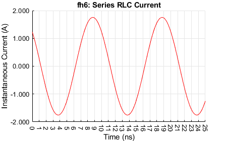
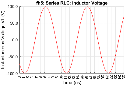
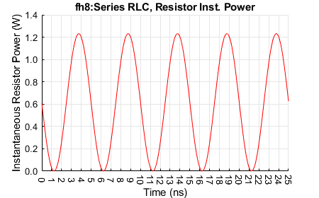
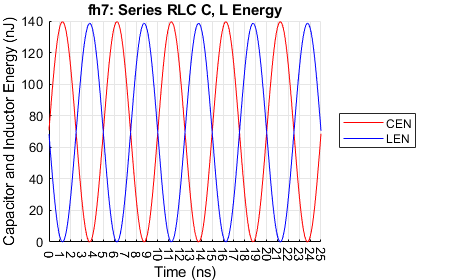
To illustrate some of the features of (unloaded) resonant circuits, some examples of AC voltages and currents around the schematic circuit of Figure 2-9 were simulated using Matlab®. These are shown in Figure 2-10 for the resonant frequency of 100 MHz and in Figure 2-11 for the lower -3 dB band edge of 99.9 MHz. Similar results were observed for the upper (-3 dB) band edge of 100.6 MHz, but are not shown. The following is a summary of the parameters used.
- Peak applied voltage (Thevenin source): 1 V
- Combined series loss resistance \(R_{LCS}\): 0.4 Ω
- Capacitance \(C\): 28 pF
- Capacitance Q-factor \(Q_C\):220
- Inductance \(L\):90 nH
- Inductance Q-factor \(Q_L\):400

Overall instantaneous current.
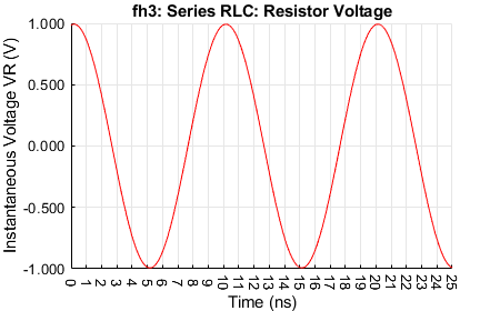
Resistor voltage.

Capacitor voltage.
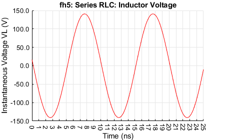
Inductor voltage.

Resistor power.
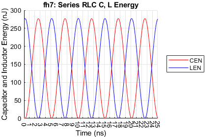
Inductor and capacitor energies.
For the resonance condition, the peak voltage across the loss resistance \(R_{LCS}\) is is 1 V, consistent with the phase voltages across \(L\) and \(C\) 'cancelling' (the same magnitudes at about 140 V but \(\pi / 2\) radians out of phase). The \(R_{LCS}\) voltage is in phase with the current. The \(C\) voltage lags the \(R\) voltage by \(\pi / 2\) radians (approximately 2.5 ns) and the \(L\) voltage leads the \(R\) voltage by \(\pi / 2\) radians radians. The resistor power peaks to about 2.5 W, consistent with an applied peak voltage of 1 V and series resistance of 0.4 Ω at resonance. The \(L\) and \(C\) energies alternate every half cycle (5 ns), in each peaking to about 275 nJ.
Figure 2-11, are the same voltages as shown in Figure 2-10, but at the -3 dB point off resonance, confirmed by the resistor peak power at about 1.25 W compared to 2.50 W at resonance.
Current.

Resistor voltage.

Capacitor voltage.
Inductor voltage.
Resistor power.
Inductor and resistor energies.
Loaded Resonant Circuits
A resonant circuit of the type shown in Figure 2-9 is considered to be unloaded, despite it including a resistor \(R_{LCS}\). That is because \(R_{LCS}\) is an aggregate of the loss resistances of \(L\) and \(C\) which are integral features of the imperfect reactive components. If \(L\) and \(C\) were considered to be ideal, \(R_{LCS}\) would be zero and the circuit would not only be completely impractical but virtually impossible to analyse because the Q-factor would be infinity and the bandwidth would be zero.
Before a resonant circuit such as this is useful it must be connected to something or 'loaded', for example as part of a filter or an oscillator. When loaded, the Q-factor of the, now loaded, resonant circuit is degraded substantially from its unloaded value and it is said to become more heavily 'damped'. The loaded resonant circuit, represented as a two port network, would normally be loaded in some way both at the input and the output. One example using a Thevenin equivalent circuit is shown in Figure 2-12. In this, the input and output ports of the resonant network are defined as 1 and 2 respectively. The input is loaded with a source impedance \(Z_S\) and the output is loaded with a load impedance \(Z_L\). For resonant circuits used in oscillator circuits, sometimes there may be no explicit input port loading, other than a resistor. The thermal or additive white Gaussian noise (AWGN) generated by the resistor may actually be used as the signal source. Although AWGN itself is a wideband source, the intention of the resonant circuit is to reduce this to a narrow band. The low power filtered AWGN at the output of the resonant network would typically then be amplified externally. In this case, \(Z_L\) would be the input impedance of the amplifier.
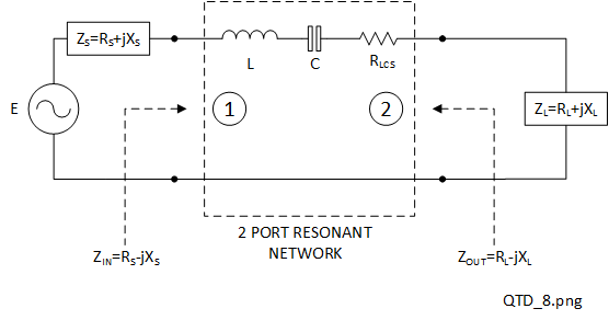
In Figure 2-12, the input and output interfacing is achieved using conjugate matching, to \(Z_S = R_S + j X_S\) at the input and to \(Z_L = R_L + j X_L\) at the output. This requires the input and output network impedances, \(Z_{IN}\) and \(Z_{OUT}\) to be the conjugates of \(Z_S\) and \(Z_L\) respectively as shown.
This is where the RF circuit design challenges begin. For many common cascaded networks, the resistive elements of the source and load impedances, \(R_S\) and \(R_L\) respectively are of the order of perhaps 20 \(\Omega\) to 150 \(\Omega\). Values like these would significantly reduce the effective Q-factor of this circuit. However, some controlled reduction in Q-factor may be useful if, for example, some tuning capability was required [13].
Loss Tangent
Like Q-factor, loss tangent is also a measure of how much the behaviour of a real reactive component, a capacitor or an inductor, departs from that of a perfect component. Loss tangent has the reciprocal behaviour to Q-factor: the smaller the loss tangent is, the closer the reactive component is to its ideal form. As the frequency is increased, high frequency degradation effects become apparent and the loss tangent inceases, or the Q-factor reduces [1] [4] [7].
Although loss tangent mathematically applies to both inductors and capacitors, it is more commonly used for capacitors, or more generally, the imperfect dielectric materials that may be modelled using parallel plate capacitors. For example, the substrate materials used for RF and microwave circuits, of which popular examples are 'FR4' and alumina. The most significant degradation of capacitor performance at higher frequencies is dominated by the dielectric properties. There will be further degradation caused by the conductive materials used for the capacitor electrodes and connectors. Copper, silver and gold have high conductivities and gold, although expensive, has the very useful property of being highly resistant to corrosion [3] [12].
For relatively low frequencies, one way of measuring the high frequency dielectric properties of a piece of unetched substrate material, double sided with parallel copper planes, is to approximate it to a parallel plate capacitor. An example is shown in Figure 2-13. The copper planes act like plates or electrodes and may be connected to a transmission/reflection measuring instrument such as a vector network analyzer (VNA). Uncertainties caused by fringing effects of the electric field in the dielectric may be minimised by choosing a thickness (plate separation) that is small compared to the electrode dimensions. The VNA must be set up to measure across an appropriate frequency range and calibrated accurately.

An ideal capacitor would have electrodes comprising formed with perfect conductors and a dielectric material formed from a perfect insulator. In a real example, neither of course would be perfect. Furthermore, the electrical characteristics of both the electrodes and dielectric will vary with frequency, similarly to how we examined the Q-factor for a real capacitor in Section 2.1.1.
One way to study the loss tangent for a capacitor is to take a quasi-static approach at low frequencies. This will typically be adequate up to a few hundred megahertz but will start to fail moving into microwave frequencies. In this, again we represent the real capacitor as an ideal capacitor connected in parallel with a resistor \(R_{CP}\) which represents the equivalent 'leakage' resistance. The leakage resistance will be partly a function of frequency from phenominia such as the skin effect in the electrodes and also contributions from the absorptive properties of the dielectric material. The rectangular geometry formed by the dielectric is consistent with that for the parallel plate capacitor and a block of bulk conductive material forming the leakage resistance. The dimensions of the dielectric material and the high value resistance formed by the imperfect dielectric will be equivalent.
The following equations represent the quasi-static relationships. (2-26) is the capacitance of the parallel plate capacitor, (2-27) is the resistance related to the conductivity and resistivity of the dielectric material [11] [12].
Using (2-26), (2-27) and the fact that the loss tangent \(\tan{\delta} \) is the reciprocal of the associated Q-factor, as shown in Figure 2-1, \(\tan{\delta} \) is given by (2-28).
The symbols used in equations (2-26), (2-27) and (2-28) are listed below:
- \(C\) is the capacitance in farad (\(F\)).
- \(R\) is the parallel resistance in ohm (\(\Omega\)).
- \(A\) is the cross sectional area of the electrodes in metre squared (\(m^2\)).
- \(t\) is the separation of the electrodes in metre (\(m\)).
- \( \epsilon_0 \) is the free space permittivity \(8.85 \times 10^{-12} \) in farad per metre (\(F / m\)).
- \( \epsilon_r \) is the relative permittivity or dielectric constant (unitless).
- \(\sigma\) is the conductivity of the dielectric material in siemen per metre (\(S / m \)).
- \( \rho \) is the resistivity of the dielectric material in ohm meter (\(\Omega m \)).
References
- Hall, Stephen H., Heck, Howard L.; Advanced Signal Integrity for High-Speed Digital Designs (Skin Depth); John Wiley & Sons Inc., New Jersey, USA; pp 204 - 218. ISBN 978-0-470-19235-1 (2009);
- Pozar, David M. (Q-factor and Resonators); Microwave Engineering - Third Edition; John Wiley & Sons Inc.; pp. 266 - 272. ISBN 0-471-44878-8 (2005).
- Pozar, David M. (op. cit.); (Conductivities and Dielectric Constants); p. 687.
- Pozar, David M. (op. cit.); (Skin Depth); pp. 18 - 19.
- Ramo, Whinnery and Van Duzer; Fields and Waves in Communication Electronics; John Wiley & Sons; pp. TBA ISBN 0-471-70721-X; pp 249 - 254 (skin effect); pp 10 - 13 (resonance & Q-factor).
- Kraus, John D. and Carver, Keith R.; Electromagnetics, Second Edition; McGraw-Hill Kogakusha Ltd.; pp. 7 - 13. ISBN 0 07 035396 4
- Hall, Stephen H., Heck, Howard L. (op. cit.); pp. 256 - 257.
- Green, Estill I.; The Story of Q; Bell Telephone System, Technical Publications Monograph 2491; Bell Telephone Laboratories Inc.; American Scientist; Vol. 43; pp. 584 - 594 (October 1955).
- US Patent 1,628,983: Electrical Network; K. S. Johnson; Electrical Networks; Patented May 17, 1927; United States Patent Office; Application filed July 9, 1923; Serial No. 650,288
- Hayt, William H.; Engineering Electromagnetics, Fourth Edition; McGraw-Hill; pp 398 - 405 (skin depth and penetration depth).
- Kraus, John D. and Carver, Keith R. (op. cit.); Parallel Plate Capacitors; pp. 49 - 50.
- Kraus, John D. and Carver, Keith R. (op. cit.); Conductivity Equation; pp. 114 - 117.
- Pozar, David M. (op. cit.); Conjugate Matching; pp. 78 - 79.
- Coilcraft Application Notes: Testing Inductors at Application Frequencies (119-3); Measuring SRF (363-1); Selecting RF Inductors (671); Inductor SPICE Models (1709/1710).
- Coilcraft Document 720-1 to 720-3.Square Air Core Inductors 1515SQ, 2222SQ, 2929SQ.
- Johanson TechnologyMulti-Layer High-Q Capacitors, S, L and E Series; pp 1-17.
- Kyocera-AVX Ultra-Broadband Resistors; UBR Series.
- Murata GJM Series High Q Multilayer Ceramic Capacitors;