How much of a digital receiver is actually analog?
First of all, what do we actually mean by a digital receiver (DRx)? We will assume that the input to the DRx comes from a digitally modulated source, therefore occupying one or more sections of the radio frequency (RF) spectrum. As it is modulated, at this point its frequency spectrum would not be at 'baseband' and would typically come from waves propagated through the atmosphere and 'collected' by an antenna. Within the DRx, signals routed from the input connector up to the associated analog to digital converter (ADC) are actually, by definition of the ADC itself, analog. By a similar argument, the signals from the output of the ADC onwards are actually digital. They would usually remain in digital form until they exited the DRx unless for some reason they encounter a digital to analog converter (DAC). So a DRx of the type we are considering would typically include both analog and digital signals of various types.
Digitally modulated waves like these which propagate through the atmosphere and use antennas may be described using the adjective 'wireless', which of course means 'no wires'. One example of a typical 'cable' input to a DRx receiver would meet one of the DOCSIS specifications. DOCSIS was developed for upgrading the former cable TV (CATV) receive only infrastructure to carry bi-directional (broadband) services for customers, mostly for internet access. DOCSIS cables do not carry digital basebands but bandwidth modulated spectra using similar techniques to those used for wireless but with different frequency ranges and powers.
As the output of an ADC is digital, for the subsequent circuits we may use suitable digital signal processing (DSP) hardware and program these with a toolbox of DSP applications in the form of software (SW) or firmware (FW). Many of these are availble in open source form, or we may prefer to write our own dedicated SW code to generate the FW. FW designed with the necessary functions may be programmed into the flash memory of the internal processor and used as required. The SW and FW used in these ways have collectively become known as software defined radio (SDR). SDR is a relatively new technology and provides routes to quickly re-configure or upgrade the DRx hardware for new frequencies, types of modulation and other parameters, provided that the hardware can accommodate the changes. Previously these would have always required hardware changes, upgrades or replacement. In fact, virtually everything which was previously done in hardware can now be done, in theory at least, with SW. The constraints are usually cost, development time, physical size/mass and reliability.
Let us examine some of the possible ADC front end configurations for a DRx. Figure 1-1 shows a simple first Nyquist zone (analog baseband) sampling configuration. Can we use something like this for all the necessary frequencies that might be received at the antenna?

The short answer is 'not yet for probably a few years' (9). Note that here we are discussing baseband sampling, either at the Nyquist sampling frequency itself (fs) or at a somewhat higher frequency with some level of over-sampling. Alternatives to this are bandpass sampling or under-sampling which are discussed with Nyquist zones in Section 10. The LPF is ideal and assumed to have a perfect 'brick wall' transmission response to reject any analog frequency components greater than one half of the ADC sampling (or Nyquist) frequency, fs/2. This is necessary to prevent aliasing.
For example, using baseband sampling, if we wanted to receive frequencies from an antenna up to 1 GHz, which covers not only several digital cellular services, but numerous others, the sampling frequency (fs) would need to be at least 2 GHz. That is quite a tall order with the present technology and a very expensive ADC option. Also, if we used this only for digital cellular services, the ADC, although being capable of converting a range of lower frequency services as well, these would not be required so the available ADC bandwidth would be wasted. The only real advantage of this design is that the circuit is simple and there is no frequency conversion or demodulation prior to the ADC.
Using a low noise amplifier (LNA) like that shown in Figure 1-1 at the front end of a receiver, especially for wireless signals, is useful provided the LNA is specified correctly. To make it effective over the full operating frequency range of something like 1 GHz, would be challenging. It would be difficult to achieve such a large bandwidth without introducing potential problems including: harmonics, intermodulation and cross modulation.
A more popular architecture is shown in Figure 1-2 for receiving quadrature amplitude modulation (QAM), probably the most common form of digital modulation.

This is known as a homodyne or zero IF front end because, for QAM, the local oscillator (LO) frequency fLO is normally tuned to the frequency at the center of the service provider's frequency spectrum. It is designed for a relatively narrow range of frequencies received at the antenna, as defined by the transmission passband of the bandpass filter, f1 to f2. For digital cellular services, this might cover a range of the allocated frequency bands, for example 900 MHz to 1 GHz. There may be several services available in this frequency range but probably only one that is required. Although the homodyne architecture has a higher part count for the analog portion than the first Nyquist zone architecture, it has several useful properties:
- The LNA is relatively narrow band and therefore should have a good noise figure (NF).
- Improved intermodulation and harmonic properties of the LNA.
- The modulated wireless waveform is directly converted to a useful quadrature (analog) baseband.
Narrow band LNAs tend to have smaller NFs than wideband LNAs because the design features and components required to increase the bandwidth are inclined to add loss to the front end of the device, which degrades its NF. Narrow band LNA performance like this will preserve or improve the DRx sensitivity.
Sometimes the BPF will be at the front end, followed by the LNA, in reverse to that shown in Figure 1-2. This has the advantage that any strong but unwanted signals near the required frequency band may be easily filtered out and thus mitigate intermodulation performance of the LNA which, after all, is not designed for high level signals. However, the in-band transmission loss of the BPF would have an equivalent NF which, in dB units, would add to the LNA NF.
If it is required to receive more than one service within the frequency range of the DRx f1 to f2, the received analog signal may be split and fed to more than one similar quadrature demodulators as shown in Figure 1-3. LO1 and LO2 may be tuned to the different service as required.

The frequencies of any unwanted wireless services present at the antenna which are well spaced from the wanted services will be outside of the LNA operating band, attenuated and be less likely to cause interference. Intermodulation and cross modulation from the LNA will be better controlled than with a wideband version.
This is the most useful property. The IQ mixer and LO are specified appropriate to the received wireless frequency. When the LO frequency (fLO) is 'tuned' to the center of the required frequency band, the action of the IQ mixer is to downconvert and demodulate (detect) the analog baseband of the service and to split this into 2 quadrature components: the in-phase (I) and the in-quadrature (Q). Each quadrature sub-band will process exactly one half of the baseband frequency range. For example, if the on-air occupied spectrum of the wireless service was 20 MHz, the bandwidth of each quadrature leg would be 10 MHz. ADC1 and ADC2 normally work in the first Nyquist zone meaning that the smallest ADC sampling frequencies, fs1 and fs2 would both be 20 MHz. A non-quadrature alternative of this is shown in Figure 1-4.
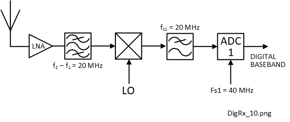
In this case, the frequency spectrum is mixed down to a baseband frequency range of 0 to 20 MHz using a good quality double balanced mixer (DBM). The baseband is low pass filtered before the ADC which uses a sampling frequency of 40 MHz. In this case the digital baseband would require further processing to extract the quadrature components.
In summary, perhaps the main advantage of using the quadrature form of down-conversion, like the example in Figure 1-2, is that the subsequent DSP can be more readily performed using quadrature components. Quadrature is necessary to achieve the orthogonality condition which is a very useful feature in DSP.
What about the less useful properties?
- Local oscillator leakage
As mentioned earlier, the local oscillator (LO), when correctly tuned, is at the same frequency as the center of the modulated frequency spectrum. If the IQ mixer does not have sufficiently good LO to RF isolation, the LO can leak in the opposite direction to the signal and even radiate from the antenna causing a potential EMC emissions problem. If a reflective object (target) is near the antenna, it may reflect these emissions and behave like a frequency modulated CW (FMCW) radar. If the target moves this could cause a DC or low frequency component tending to rotate the IQ constellation.
What determines the necessary data channel bandwidth?
Several factors need to be taken into account to determine the bandwidth necessary to carry a data channel. Some of these are listed below.
- Regulatory approval (licensing)
- The overall data throughput information rate
- Coding overheads for error detection/correction and security (encryption/decryption)
- Future expansion
- Baseband waveforms
All wireless services require to be licensed in some way to control interference, comply with international standards and to generate revenue. As wireless transmissions (radio waves) are capable of crossing borders and causing interference in other countries the licensing conditions are agreed amongst the vast majority of countries with few exceptions. Even so-called 'unlicenced' frequency bands, such as those used by equipment operating in the industrial, scientific and medical (ISM) frequency bands, is effectively licenced but by the manufacturer, not the owner or user. The manufacturer is required to verify and validate the performance of the equipment and the user must comply with the correct ownership and operating conditions, such as not modifying the equipment in any way, like using an additional amplifier or a directional antenna.
The licence conditions will specify the frequency spectrum or spectra that may be used together with other parameters such as operating specification, modulation, EIRP etc. The occupied spectrum will therefore be clearly defined with strict limits of unintentional radiation, radiated and conducted emissions.
One of the results of the Shannon Hartley capacity theorem is that, for the same Eb/N0 faster information rates require proportionally larger bandwidths. However, there are many ways that the digital data in a baseband may be represented using discrete voltage levels by pulse amplitude modulation (PAM) (14). These are represented by ones and zeros or marks and spaces, respectively. Some examples of these are shown in Figure 2-1.
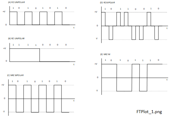
We wish to represent each bit in a stream of binary data by one of 2 possible voltage states for a defined length of time. Alternatively we may represent them by changes in voltage states. In fact there are many ways that we may represent data streams by voltage levels. Perhaps the most common are return to zero (RZ) and non-return to zero (NRZ) and examples of each are shown in Figure 2-1. The positive, negative and zero voltage states are shown and, as their names imply, for RZ, one of the waveform voltage states is zero and for NRZ, no voltage state is zero. Waveforms A and B are RZ unipolar, meaning that there is one state other than zero. Waveforms C, D and E are bipolar, there being two voltage states other than zero.
Content under construction, expected delivery July 2021
Content under construction, expected delivery July 2021
Content under construction, expected delivery July 2021
What parameters define the performance of a digital receiver?
The digital receiver (DRx) comprises both analog and digital parts, so there are both analog and digital properties to define. Some of these include the following:
- Frequency ranges and synthesizer resolution.
- Modulation properties, coding and information rates.
- Input power handling and AGC capability.
- Simultaneous multi-service capability.
- Susceptibility to interference, conducted and radiated.
- Emissions of interference, conducted and radiated.
- Phase noise.
- SDR capability and upgradability.
- Overload capability: wanted signals and impulse (lightning).
- Latency.
- Electrical interfaces.
- Physical interfaces.
- Noise figure.
- Power supply requirements.
- Physical chartacteristics.
- Power Interface and Temperature Requirements.
How does the Shannon Hartley capacity theorem relate to digital receivers?
The Shannon-Hartley capacity theorem relates to a bandwidth limited digital communication channel in the presence of additive white Gaussian noise (AWGN) (2). AWGN was chosen because it is inherent in the hardware itself and is a function of the product of only two parameters: the absolute temperature of the hardware and the noise bandwidth of the channel. The Shannon-Hartley capacity of the channel is the maximum theoretical data rate that such a channel will support, given its bandwidth and signal power. The formula for this is given by (4-1).
where, for the channel:
- C is the Shannon-Hartley capacity (bit/s)
- B is the noise bandwidth (Hz)
- S is the mean signal power (W)
- N is the mean noise power (W)
With the Shannon-Hartley channel capacity theorem there are no restrictions on data rate, parity, forward error correction, modulation or any other feature of the channel that we might want to deploy to improve its error performance. As long as sufficiently error-free data is successfully transmitted, even if the net data throughput is one bit per week, it will still be compliant with the theorem. Now we will define some other important parameters.
The energy per bit (Eb) is the mean signal power of the digital signal divided by the actual data rate (R) (4-2).
where:
- Eb is the energy per bit (J)
- R is the actual data rate through the channel (/s)
It is useful to normalise the total mean noise power in the channel against its (noise) bandwidth (4-3).
where:
- N0 is the noise power density (W/Hz)
The limit of operation of the channel is when the data rate is equal to the channel capacity, C=R. Substituting for this, also for S and N from (4-2) and (4-3) respectively, gives (4-4).
γ=R/B is a measure of the theoretical utilisation efficiency of the channel in bit/s/Hz (4-5).
A useful way of representing this information graphically is to plot the utilisation factor from (4-6).
The plot in Figure 4-1 is of gamma (γ) against 10log10(Eb/N0). Note that γ does not have any units but the variable Eb/N0 has been converted to the logarithmic (decibel) form so here it has units of dB. However, to further confuse things, the Eb/N0 dB values have been scaled linearly and the γ values logarithmically to base 2.

Plots of this type derived from the Shannon Capacity theorem are some of the most important in communications theory. The y axis (γ) is the ratio of data rate to the associated bandwidth necessary to transmit that bandwidth, with units of bits per second per hertz (bit/s/Hz). This is sometimes referred to as the utilisation factor. The x axis is the ratio of energy per bit to noise power density which here, as we mentioned, is in logarithmic (dB) units. The plot represents the theoretical limit of possible communications through a channel limited only by AWGN. This is independent of the data rate or any type of error correction which may be used. If the dB value of Eb/N0 is less than the Shannon limit of -1.6 dB, communications will be impossible whatever form of error mitigation we try (2). The Shannon limit therefore serves as a goal in designing digital communications equipment, one which we know will never be equalled. However, the closeness a piece of equipment to the Shannon limit provides a measure of the current technology and the quality of its design. In the years since Shannon's work in 1948, the practical and achievable performances of digital receivers have come to within about 2 dB of the Shannon limit helped with the use of turbo codes (2).
The RF spectrum is a valuable but restricted resource shared across the World and sections of it are traded as an expensive commodity between service providers and government controlled communications regulators. Perhaps the clearest evidence of this is in the expansion of the analog and later digital cellular communications infrastructure starting in the 1980s. Therefore most service providers' first instinct is to demand whatever is necessary to achieve the largest possible channel capacity in the smallest possible bandwidth: what we referred to earlier as the utilisation factor (γ). From Figure 4-1 we can see that this would require ever increasing values of Eb/N0, which is analogous to signal to noise ratio if this was an analog communications system. How can we increase Eb/N0?. Increase Eb, reduce N0 or both? From (4-2) and (4-3) we may extend this to include signal power (S), actual data rate (R), total noise power in the noise bandwidth (N) and the noise bandwidth itself (B).
So, to increase the information capacity, this gives us a tradeoff amongst competing parameters S, B, R and N. We will address each of these considered separately:
- Increase Received Signal Power (S)
- Increase the Bandwidth (B)
- Increase the Data Information Rate (R)
- Reduce the AWGN Power (N)
To increase the signal power at the receiver the power flux density (PFD) must be increased. This may be achieved with more directional antennas directed at the service area, thus avoiding power wastage outside of it and reducing the risk of interference to adjacent service areas. This may be further increased by using electronically scanned 'smart' antennas: several steerable and even narrower antenna beams which 'track' the users' locations. Also the output powers from the transmitter (for example base stations or cell towers for digital cellular services) may be increased.
The best way to achieve this is to split existing cells into smaller cells as more capacity is required, therefore creating more cells and then revise the antenna coverage and transmitter powers. Although the new transmitter powers will not require to be those of the original larger cells, they may be modified to produce increased PFDs in the new service areas.
Within Europe, The Third Generation Partnership Project (3GPP) is the standards organisation which regulates the evolution of the 2G (TDMA), 3G (CDMA), 4G(LTE/LTE-A) and the emerging 5G digital cellular services. There are similar organisations for other areas of the world. Each evolution through the generations has sought to increase the bandwidth available to service providers and users and therefore steadily increase the information capacity available to customers who have the necessary funds to pay for the services. In the latest 4G service known as Long Term Evolution, Advanced (LTE-A), wide bandwidth service are achieved using 'carrier aggregation'. This can join more than one allocated bandwidth with another, even if they are in non-contiguous frequency ranges. The greater the on-air frequency spectrum allocation is, proportionally the more bandwidth will be available. Some of the LTE-A allocations go up to around 2.7 GHz, but the emerging 5G services are allocated even higher frequencies well into the microwave frequency bands. When these service become widely operational, even more bandwidth should become available.
Increasing the data information rate requires extra bandwidth. This may be confirmed by performing a discrete FFT on the faster data compared with the slower one, assuming that they both have the same bit voltage state specification. If there was no noise, theoretically the bandwidth would extend to infinity. By definition we are including AWGN so its absolute bandwidth is limited to where its amplitude falls below that of the AWGN.
The AWGN power is a function of the product of just two parameters: the absolute temperature of the AWGN source (T) and the noise bandwidth (B). Reducing the temperature of the receiver front end (LNA) is technically possible but prohibitively expensive for competitive commercial services such as digital cellular communications. It may be an option in specialist fields such as radio astronomy. Today's technology offers low noise amplification devices such as high electron mobility transistors (HEMTs) and pseudo HEMTs (PHEMTs) which have very low AWGN noise floors and therefore low NFs.
How do we convert especially high frequencies to more manageable frequencies?
Figure 5-1 shows a schematic of a typical homodyne front end of a digital receiver. Conversion of the received frequency band, f1 to f2 to the quadrature (IQ) baseband is in one step as the LO is tuned to the center frequency of the wireless service. Components within the IQ mixer and the LO source itself will therefore require to be specified for frequencies including f2, preferably with a comfortable margin above this. In general, the part, design and production costs increase in proportion to their specified highest frequencies. However, there are usually more service bandwidths available at the higher frequencies so, until the technology progresses further, it may be cost effective to downconvert blocks of these higher frequencies down to more manageable frequencies before the next stage of conversion to the baseband frequency. The first frequency is known as an intermediate frequency (IF).
What are some more popular types of digital modulation?
Here, we are not considering baseband modulation which is sometimes used to describe the creation of a digital baseband using pulse amplitude modulation (PAM), but we are looking at bandpass modulation. A baseband spectrum starts at or close to 0 Hz, zero frequency or DC and extends to a finite upper limit. The result of bandpass modulation is a finite width spectrum usually with a center frequency which is much greater than the maximum baseband frequency. The width or bandwidth of the spectrum would typically be about twice its maximum baseband frequency. For example, the baseband waveform of a digitally modulated transmission might occupy a spectrum from 0 Hz to 1 MHz but after bandwidth modulation at 500 MHz its spectrum would range from 499 MHz to 501 MHz.
A carrier (continuous wave or CW) may be modulated in order to carry information by altering one or more of its parameters: frequency, amplitude or phase. Digital modulation is achieved by performing the modulation with discrete steps applied to one or more of the parameters. The most common form of digital modulation is quadrature amplitude modulation (QAM) in which both the amplitude and the phase of the carrier are modulated. It is a 'M-ary' form of modulation meaning that it may have different orders 'M' each of the form M-QAM, where:
In QAM, the number of available discrete amplitude and phase values is known as the symbol set, equivalent to the order (M). Each symbol is made up of k bits so it is simple to convert from bits to symbols at the transmit end and vice versa at the receive end. The symbol sets may be represented as voltages on IQ axes by a constellation of dots, each dot representing one symbol's position in terms of amplitude and phase. The quadrature (IQ) axes also relate very conveniently to the quadrature architecture used in the homodyne front end, Figure 5-1. Some examples of these are shown in Figure 6-1.

The QAM constellation diagrams shown are for 2-QAM (or binary phase shift keying, BPSK), 4-QAM (or quadrature phase shift keying, QPSK) and 64-QAM. For the related discussion we will assume that these constellation diagrams are to the same (voltage) scale. By convention, the horizontal axis is the in-phase (I) component and the vertical axis is the in-quadrature (Q) component. From (6-1), the number of bits per symbol (k) are 1, 2 and 4 respectively and the number of available symbols are 2, 4 and 16 respectively. Thus, the higher the QAM order is the closer each symbol will be to its next closest symbol. This means that once we allow for additive white Gaussian noise (AWGN), the higher order constellations have a greater probability of errors. The least error prone is 2-QAM, more commonly referred to as BPSK.
BPSK is the most resistant QAM order to AWGN because it comprises the smallest possible symbol set of 2.The voltage amplitudes of both symbols are equal, usually normalised to 1 V and they have a phase difference of 180°. As an example of BPSK in the time domain, Figure 6-2 shows the voltage time waveform of 6 consecutive symbols at a BPSK modulator output for a carrier (local oscillator) frequency of 10 MHz. If the probabilities of either a 1 or a 0 are both equal at 0.5, ther average frequency will be 10 MHz.

For BPSK there is one bit per symbol and the amplitude of the modulated waveform remains constant, 1 V being chosen for this example. In this case a phase of zero represents a symbol of 1 and a phase of 180° represents a symbol of 0. The waveform shown is for 6 symbols 100101 starting at the most significant bit (MSB). In this case, 2 LO cycles are used for each symbol, so the duration of each is 200 ns.
Digital baseband waveforms for pulse amplitude modulation
The word 'baseband', or 'digital baseband' in the case of digital communications, refers to a frequency spectrum, the result of digital modulation, which covers a range from at or near zero (DC) to some defined upper limit (14). The upper limit could range from around 1 MHz for a low capacity system to many gigahertz for some high capacity telecommunications infrastructure equipment.
A common baseband modulation is pulse amplitude modulation (PAM). As its name implies, PAM is the process of representing the binary data (bit) stream to be transmitted by discrete (amplitude) voltage levels, or pulses. There are many ways that this could be achieved, but common forms of PAM are 'return to zero' (RZ) and non-return to zero (NRZ). For RZ, the bit waveform will settle for some finite time at 0 V and for NRZ it will never settle at 0 V but may almost instantaneously pass through 0 V. Both RZ and NRZ can be unipolar or bipolar forms. Unipolar means that each bit waveform has one voltage state other than 0 V and bipolar refers to it having two states other than 0 V. The zero state in the bipolar form is not a 1 or 0 detection state and the bipolar voltages are symmetric with a mean value of zero.
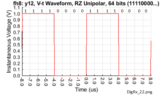
Some alternative RZ baseband waveforms for streams of periodic digital data are shown in Figure 7-1, Figure 7-3, Figure 7-5 and Figure 7-7. The first of these is a RZ unipolar waveform with a 1 state of +1 V and a 0 state of 0 V. This is shown in Figure 7-1 carrying a long string of alternating of 1s and 0s. The pulse or bit width is 1 µs so the data information rate or signaling rate is 1 Mbit/s.

This waveform is equivalent to a periodic rectangular waveform with a frequency of 500 kHz and a duty ratio of 50% or, more simply, a square wave of frequency 500 kHz. It also has a peak to peak amplitude of 1 V and a long term mean value of 0.5 V.
In theory, the content of a digital stream could contain all 0s, all 1s or any mixture of 1s and 0s, with the highest frequency content for this repeating '1010' waveform. However, if long strings of the same bit are possible, this can cause issues with a significant build up of a DC component, sometimes called 'DC wander', in this case either 0 V or 1 V. Often the coding is therefore designed to deliberately introduce state transitions to avoid this from happening. The spectrum for the RZ unipolar '1010...' waveform shown in Figure 7-1 is shown in Figure 7-2. This was generated using the fast Fourier transform (FFT) function in Matlab®.

This shows a DC or 0 Hz component with an ampllitude at 114 dBuV, which converts to a linear value of 0.5 V. This is consistent with the average value of the 50% duty cycle waveform for many cycles of the waveform shown in Figure 7-1. The remaining parts of the FFT result provide a guide to the maximum frequency content of the baseband spectrum with discrete components starting at 500 kHz with 1 MHz spacing. We will now extend the same RZ unipolar waveform to one comprising alternate groups of 4 1s followed by 4 0s and so on, the waveform shown in Figure 7-3.
So, in this case the DC component is unchanged, the smallest discrete components are 250 kHz and the spacing is 500 kHz. Compared to Figure 7-1, Figure 7-3 has a period and pulse width of four times the value so the fundamental frequency is one quarter of the previous value. The FFT of this waveform is shown in Figure 7-4.

Compared to the RZ unipolar waveforms, an example of an RZ bipolar waveform is shown in Figure 7-5. The peak to peak voltage and bit width for this waveform were the same as those in the RZ unipolar waveforms, chosen for comparison purposes.

The waveform for each bit is a high to low transition for a 1 and a low to high transition for a 0, each state being one half of a bit width. Therefore, the average voltage for a 1 is +0.25 V and for a 0 is -0.25 V. So a long string of 1s or 0s, if either was allowed, would generate average voltages of these respective values. However, for an average data throughput, the probability of either a 1 or a 0 occurring is usually about 0.5, so the average waveform voltage should be close to 0 V. A small average voltage reduces the risk of DC voltages building across coupling capacitors, inadvertently biasing the datastream and causing detection errors. The FFT for this waveform is shown in Figure 7-6.

Clearly there is no DC component, nor would we expect one, as the average voltage for a data stream of many bits is 0 V. Another important advantage of the RZ bipolar waveform is that it creates a significant and consistent frequency spectrum components, in this case starting at 500 kHz and increasing with 1 MHz spacing. These support synchronous communication systems in which the clock is extracted from the data.
For completeness, Figure 7-7 shows the RZ bipolar waveform but carrying alternative groups of 4 ones followed by 4 zeros.

The FFT of this waveform is shown in Figure 7-8 with an expanded frequency scale to emphasise the frequency spacing of the discrete components.

There is clearly no DC component as we would expect with a long term average being 0 V. For each side of the spectrum, the first discrete is at 250 kHz and the spacing is 500 kHz.
How do SNR and Eb/N0 influence a digital receiver performance?
Figure 8-1 shows a NRZ bipolar baseband waveform with the 1 and 0 states of +1 V and -1 V respectively with superimposed additive white Gaussian noise (AWGN).

AWGN, by definition, has a Gaussian distribution of the noise voltage amplitude over time. This will be added to the digital voltage state as shown in Figure 8-1. Therefore, there is a finite probability that the instantaneous magnitude of the noise voltage will sometimes be quite high. It might even exceed the threshold for the unintended bit and cause an error should the noisy waveform be sampled at that point.
In order to calculate the probability of errors occuring on a baseband NRZ bipolar waveform which is subject to AWGN, Figure 8-2 shows how the Gaussian probability density functions (PDFs) for each of the states may be used.
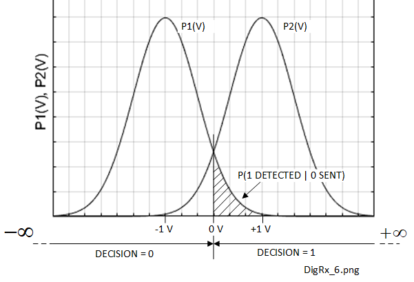
This is a fundamental application of conditional probability summarised in Bayes' Theorem. In this case we assume that the probability of receiving a 1 is equal to that for receiving a 0, or 0.5 in each case. Then the shaded area under the Gaussian PDF curve gives the probability of detecting a 1 if a 0 was sent. Both values of probability are included in Bayes' theorem to get the result.
What are IQ mixers and how are they used?
An 'IQ' mixer refers to an in-phase, in-quadrature mixer. IQ mixers are frequently used in digital receivers as demodulators and in digital transmitters as modulators. Circuit schematics for each of these are shown in Figure 9-1 and Figure 9-2 respectively.


IQ mixers are analog components normally found before the ADC in a digital receiver or after the DAC in a digital transmitter. They work on the principle of splitting a continuous wave (CW) local oscillator into 2 quadrature (90° separated) components, I and Q which represent the real and imaginary axes respectively of an argand diagram. This may be achieved with a quadrature splitter appropriate for the LO frequency. A vector or phasor on the argand diagram may be used to describe the amplitude (length) and spatial phase (angle) of the carrier. By convention, in the argand diagram, the I and Q quadrature components are represented by the x and y axes respectively.
Each of the I and Q (quadrature) components is fed to one port of a double balanced mixer (DBM). The DBM is shown schematically in Figure 9-3.

This version of DBM shows the use of 3 transformers, each one providing a single ended port to interface external components to the inner balanced circuits. Ports 1 and 2 may be used for the LO and signal to be processed and port 3 provides the analog IF input for a modulator or output for a demodulator. At the higher microwave frequencies, wire wound transformers would not be appropriate but there are alternative circuit based solutions and distributed components which can provide similar functions.
The balanced circuit topology of the DBM means that the LO component applied at port 1 should theoretically be completely suppressed and none should leak out of port 2 or port 3. However, it is difficult to achieve perfect balance and a few balance imperfections will probably cause some LO leakage from these ports.
The IQ mixer IF ports (port 3 in each case) provide the I and Q baseband components from the demodulator or receive them for the modulator. The other IQ mixer component is a zero degrees combiner or splitter. This may well be a similar physical design to the quadrature combiner/splitter but of course without the π/2 phase changing component.
What do you mean by 'Nyquist zones', oversampling and undersampling?
Nyquist's sampling criterion requires that the sampling frequency (fs) must be at least twice the maximum frequency component that is present in the baseband spectrum (fa). To confirm this we often assume that there is an ideal or 'brickwall' low pass filter (LPF) before the analog input of the ADC as shown in Figure 10-1. This colloquial term refers to a theoretical filter which, for a LPF, has 100% transmission in-band and zero transmission out of band. The Nyquist frequency is defined as fs/2.

In general, it is good practice to increase the sampling frequency to somewhat above twice fa which is known as over sampling. This will provide a margin to accommodate the finite LPF attenuation roll-off seen in real life to minimise aliasing and to simplify its design. Sometimes the sampling frequency may even be several times the Nyquist frequency. This may generate digital data which is not required but the data concerned may simply be ignored, by a process of decimation later in the DSP chain. The main tradeoff required for over sampling is that the ADC and DSP stages must be specified for the higher sampling frequency and necessary information rate. These requirements will add extra design and parts costs.
Until now we have been considering baseband sampling within the Nyquist criterion, fs≥2fa. A study of the sampling process itself and how this generates pulse amplitude modulation (PAM), also shows that it generates higher order Nyquist zones in the frequency domain (6) (5). These may be exploited to achieve sampling across bands of frequencies, every component of which, is actually greater than the sampling frequency itself. Not surprisingly, this process is called undersampling or bandpass sampling.
There are various sampling methods but, to a reasonable approximation, the sampling (voltage time) waveform 'amplitude modulates' the baseband (voltage time) waveform.
The theoretical sampling function in the time domain is based upon a regular train of impulse, or Dirac delta δ(t) functions, equally spaced in time by the reciprocal of the sampling frequency. These are used to take regularly spaced samples of the baseband voltage time waveform as shown in Figure 10-2 (10).

In Figure 10-2, (A) shows a typical baseband voltage time waveform x(t) and (B) the impulse sampling waveform with equally spaced time impulses of interval Ts. The sampling frequency (fs) and the sampling period (Ts) have the reciprocal relationship given by (10-1)
The sampling waveform considered in isolation, xδ(t), is the discrete sum of the impulse samples from -∞ to +∞, given by (10-2) (5):
The infinite sampling range is mathematically necessary to comply with the conditions required for Fourier transforms which will be applied to get the voltage against frequency spectrum.
The function which describes the pulse amplitude modulation (PAM) in the time domain is the product of x(t) and xδ(t) (10-3).
The equations shown in (10-3) also apply the sifting or sampling property of Fourier transforms. This is shown explicitly in (10-4).
The sifting property means that the product x(t)xδ(t) may be applied at every impulse (time) location using the instantaneous value of the baseband voltage at that time. The result of this is the impulse functions in Figure 10-2 (C) which are 'shaped' or amplitude modulated by the envelope profile of the baseband waveform.
In order to arrive at the frequency spectra, we can use some standard Fourier transform (FT) properties, one of which is convolution (9). In the following equations, we use the convention that a function symbol uses lower case in the time domain and upper case in the frequency domain so, for example, X(f) is the FT of x(t). Figure 10-3 shows the spectra created by the respective time domain waveforms that were shown in Figure 10-2.

In Figure 10-3, (A) shows the baseband frequency spectrum and (B) shows the frequency components of the sampling waveform given by (10-5) which is another one of the FT properties (9).
(10-7) shows that the result of the PAM applied to the spectrum for the baseband waveform is to create repeated spectra in the frequency domain, with frequency spacing of nfs/2 where n is an integer. For the moment we will assume that the sampling frequency is precisely on the threshold at exactly twice the maximum baseband frequency. The resulting frequency spectrum is shown in Figure 10-4.

The repeated frequency spectra start with the first Nyquist zone (Z1) between zero frequency and fs/2, the same frequency range that the baseband occupies. The higher order zones Z2, Z3 and so on are then numbered serially for increasing frequency as shown in Figure 10-4, irrespective of whether they may be upper or lower sidebands. In fact, we are not generally concerned whether the zone is upper or lower sideband because the DSP processor(s) which follow the ADC may simply be programmed for either using just a very slightly different algorithm.
To achieve baseband sampling, we know that we must filter out all but the first Nyquist zone (Z1) by using a brickwall LPF covering the Z1 frequency range as shown in Figure 10-1. The LPF would reject any signals or noise present above one half of the sampling frequency to prevent aliasing.
However, a potentially very useful property of the sampled spectra, or higher order Nyquist zones is that we can instead select a higher order (bandpass) zone, let us say for the sake of argument, Z4 in Figure 10-4, and convert this using an ADC instead of the baseband zone, Z1. Figure 10-5 shows the essential input configuration to the ADC required to achieve this.

If the frequency range of Z4 was 30 MHz to 40 MHz for example, fs/2=10 MHz and the sampling frequency for this brickwall filter case would be 20 MHz.
More generally, when designing undersampling architectures some manipulation of the frequencies and a few precautions are necessary:
- The ADC must be correctly specified for undersampling
- The selected bandpass Nyquist zone order should not be too high
- The sampling frequency and Nyquist zone
Many ADCs are not actually suitable for undersampling applications. The ADC input bandwidth or frequency range must be adequately specified to accommodate both the maximum absolute frequency of the analog input waveform and the maximum sampling frequency.
One drawback of undersampling is that there will be (AWGN) noise contributions to the ADC analog input from all Nyquist zones wanted or not by a similar undersampling mechanism. For the example frequency spectrum shown in Figure 17-4, these will come from Z1, Z2, Z3, Z5 and perhaps even higher orders. Even if a high quality bandpass filter is used at the ADC analog input, this will not reject noise which may be present internal to the ADC.
We know that, with DSP, we should avoid fractional coefficients in favour of integer ones because the processing is much easier. Undersampling is no exception. We must maintain an integer relationship between the Nyquist frequency fs/2 and the bandpass sampling frequency range: say from its lower frequency fl to its upper frequency fu. Simultaneously, we have to ensure that the passband frequency range fu - fl is not greater than fs/2. Preferably it should be slightly less to accommodate a bandpass filter with a response which falls short of the brick wall ideal. This is best demonstrated with an example, one of which is described in Section 11.
An undersampling example
In keeping with some excellent tutorials, datasheets and other documentation available from Analog Devices, the following discussion is based on their tutorial MT-002.
Referring to the Nyquist frequency zone spectra in Figure 10-4, taking one of the zones of order n, covering a frequency range from fl to fu, these are related by (11-1).
By adding the two equations in (11-1), the result for n is given by (11-2).
For example, if we require fl=33 MHz and fu=41 MHz, then (11-2) gives the result n=5.125, which is clearly not an integer. Removing the fractional part provides the integer value of 5 which is required. The 'rounded down' integer value is chosen because this will increase fs/2 to slightly above the Nyquist threshold value to avoid aliasing. Then (11-2) is re-arranged in terms of fs, and the values for fl, fu and n are substituted into (11-3) to give the result, fs=16.44 MHz.
The final step is to re-calculate fl and fu from (11-1) by substituting fs=16.44 MHz and n=5. The results are 32.88 MHz and 41.10 respectively. This gives margins of 120 kHz and 100 kHz on the lower and upper frequency edges of the required bandpass filter respectively.